- 您现在的位置:买卖IC网 > PDF目录13376 > CS5171GDR8 (ON Semiconductor)IC REG MULTI CONFIG 1.5A 8SOIC PDF资料下载
参数资料
| 型号: | CS5171GDR8 |
| 厂商: | ON Semiconductor |
| 文件页数: | 11/21页 |
| 文件大小: | 0K |
| 描述: | IC REG MULTI CONFIG 1.5A 8SOIC |
| 产品变化通告: | Product Discontinuation 27/Jun/2007 |
| 标准包装: | 1 |
| 类型: | 升压(升压),回扫,正向转换器,Sepic |
| 输出数: | 1 |
| 输入电压: | 2.7 V ~ 30 V |
| PWM 型: | 电流模式 |
| 频率 - 开关: | 280kHz |
| 电流 - 输出: | 1.5A |
| 同步整流器: | 无 |
| 工作温度: | 0°C ~ 125°C |
| 安装类型: | 表面贴装 |
| 封装/外壳: | 8-SOIC(0.154",3.90mm 宽) |
| 包装: | 剪切带 (CT) |
| 供应商设备封装: | 8-SOICN |
| 其它名称: | CS5171GDR8OSCT |
�� �
�
�CS5171,� CS5172,� CS5173,� CS5174�
�Switch� Driver� and� Power� Switch�
�The� switch� driver� receives� a� control� signal� from� the� logic�
�section� to� drive� the� output� power� switch.� The� switch� is�
�grounded� through� emitter� resistors� (63� m� W� total)� to� the�
�PGND� pin.� PGND� is� not� connected� to� the� IC� substrate� so� that�
�switching� noise� can� be� isolated� from� the� analog� ground.� The�
�peak� switching� current� is� clamped� by� an� internal� circuit.� The�
�clamp� current� is� guaranteed� to� be� greater� than� 1.5� A� and�
�varies� with� duty� cycle� due� to� slope� compensation.� The�
�power� switch� can� withstand� a� maximum� voltage� of� 40� V� on�
�the� collector� (V� SW� pin).� The� saturation� voltage� of� the� switch�
�is� typically� less� than� 1� V� to� minimize� power� dissipation.�
�Short� Circuit� Condition�
�When� a� short� circuit� condition� happens� in� a� boost� circuit,�
�the� inductor� current� will� increase� during� the� whole�
�switching� cycle,� causing� excessive� current� to� be� drawn� from�
�the� input� power� supply.� Since� control� ICs� don’t� have� the�
�means� to� limit� load� current,� an� external� current� limit� circuit�
�(such� as� a� fuse� or� relay)� has� to� be� implemented� to� protect� the�
�load,� power� supply� and� ICs.�
�In� other� topologies,� the� frequency� shift� built� into� the� IC�
�prevents� damage� to� the� chip� and� external� components.� This�
�feature� reduces� the� minimum� duty� cycle� and� allows� the�
�transformer� secondary� to� absorb� excess� energy� before� the�
�switch� turns� back� on.�
�I� L�
�V� OUT�
�V� CC�
�approximately� 1.5� V,� the� internal� power� switch� briefly� turns�
�on.� This� is� a� part� of� the� CS517x’s� normal� operation.� The�
�turn� ?� on� of� the� power� switch� accounts� for� the� initial� current�
�swing.�
�When� the� V� C� pin� voltage� rises� above� the� threshold,� the�
�internal� power� switch� starts� to� switch� and� a� voltage� pulse� can�
�be� seen� at� the� V� SW� pin.� Detecting� a� low� output� voltage� at� the�
�FB� pin,� the� built� ?� in� frequency� shift� feature� reduces� the�
�switching� frequency� to� a� fraction� of� its� nominal� value,�
�reducing� the� minimum� duty� cycle,� which� is� otherwise�
�limited� by� the� minimum� on� ?� time� of� the� switch.� The� peak�
�current� during� this� phase� is� clamped� by� the� internal� current�
�limit.�
�When� the� FB� pin� voltage� rises� above� 0.4� V,� the� frequency�
�increases� to� its� nominal� value,� and� the� peak� current� begins�
�to� decrease� as� the� output� approaches� the� regulation� voltage.�
�The� overshoot� of� the� output� voltage� is� prevented� by� the�
�active� pull� ?� on,� by� which� the� sink� current� of� the� error�
�amplifier� is� increased� once� an� overvoltage� condition� is�
�detected.� The� overvoltage� condition� is� defined� as� when� the�
�FB� pin� voltage� is� 50� mV� greater� than� the� reference� voltage.�
�COMPONENT� SELECTION�
�Frequency� Compensation�
�The� goal� of� frequency� compensation� is� to� achieve�
�desirable� transient� response� and� DC� regulation� while�
�ensuring� the� stability� of� the� system.� A� typical� compensation�
�network,� as� shown� in� Figure� 31,� provides� a� frequency�
�response� of� two� poles� and� one� zero.� This� frequency� response�
�is� further� illustrated� in� the� Bode� plot� shown� in� Figure� 32.�
�V� C�
�R1�
�V� C�
�CS5171�
�C1�
�C2�
�GND�
�fP1� +�
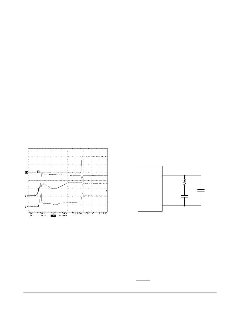
�Figure� 30.� Startup� Waveforms� of� Circuit� Shown� in�
�the� Application� Diagram.� Load� =� 400� mA.�
�The� CS517x� can� be� activated� by� either� connecting� the�
�V� CC� pin� to� a� voltage� source� or� by� enabling� the� SS� pin.�
�Startup� waveforms� shown� in� Figure� 30� are� measured� in� the�
�boost� converter� demonstrated� in� the� Application� Diagram�
�on� the� page� 2� of� this� document.� Recorded� after� the� input�
�voltage� is� turned� on,� this� waveform� shows� the� various�
�phases� during� the� power� up� transition.�
�When� the� V� CC� voltage� is� below� the� minimum� supply�
�voltage,� the� V� SW� pin� is� in� high� impedance.� Therefore,�
�current� conducts� directly� from� the� input� power� source� to� the�
�output� through� the� inductor� and� diode.� Once� V� CC� reaches�
�Figure� 31.� A� Typical� Compensation� Network�
�The� high� DC� gain� in� Figure� 32� is� desirable� for� achieving�
�DC� accuracy� over� line� and� load� variations.� The� DC� gain� of�
�a� transconductance� error� amplifier� can� be� calculated� as�
�follows:�
�GainDC� +� GM� RO�
�where:�
�G� M� =� error� amplifier� transconductance;�
�R� O� =� error� amplifier� output� resistance� ≈� 1� M� W� .�
�The� low� frequency� pole,� f� P1,� is� determined� by� the� error�
�amplifier� output� resistance� and� C1� as:�
�1�
�2� p� C1R� O�
�http://onsemi.com�
�11�
�相关PDF资料 |
PDF描述 |
|---|---|
| ABC25DREN | CONN EDGECARD 50POS .100 EYELET |
| GSC31DRTN-S13 | CONN EDGECARD 62POS .100 EXTEND |
| ECM24DRAN | CONN EDGECARD 48POS R/A .156 SLD |
| GMC31DRTN-S13 | CONN EDGECARD 62POS .100 EXTEND |
| MAX706APESA+T | IC SUPERVISOR LOW COST 8SOIC |
相关代理商/技术参数 |
参数描述 |
|---|---|
| CS5171GDR8G | 功能描述:直流/直流开关调节器 1.5A High Efficiency Boost RoHS:否 制造商:International Rectifier 最大输入电压:21 V 开关频率:1.5 MHz 输出电压:0.5 V to 0.86 V 输出电流:4 A 输出端数量: 最大工作温度: 安装风格:SMD/SMT 封装 / 箱体:PQFN 4 x 5 |
| CS5171HVBSTGEVB | 制造商:ON Semiconductor 功能描述:P2 - DCDC CONVERSION - Bulk |
| CS5172/4_EVM_INVERT | 制造商:ON Semiconductor 功能描述:CS5172/4 eval board 制造商:ON Semiconductor 功能描述:1.5 A 280 kHz/560 kHz Boost Regulators |
| CS5172_EVM_FLYBACK | 制造商:ON Semiconductor 功能描述:1.5 A 280 kHz/560 kHz Boost Regulators 制造商:P&S 功能描述:1.5 A 280 kHz/560 kHz Boost Regulators |
| CS5172ED8 | 功能描述:直流/直流开关调节器 1.5A High Efficiency RoHS:否 制造商:International Rectifier 最大输入电压:21 V 开关频率:1.5 MHz 输出电压:0.5 V to 0.86 V 输出电流:4 A 输出端数量: 最大工作温度: 安装风格:SMD/SMT 封装 / 箱体:PQFN 4 x 5 |
发布紧急采购,3分钟左右您将得到回复。