- 您现在的位置:买卖IC网 > PDF目录13335 > CS5172ED8 (ON Semiconductor)IC REG MULTI CONFIG 1.5A 8SOIC PDF资料下载
参数资料
| 型号: | CS5172ED8 |
| 厂商: | ON Semiconductor |
| 文件页数: | 15/21页 |
| 文件大小: | 0K |
| 描述: | IC REG MULTI CONFIG 1.5A 8SOIC |
| 产品变化通告: | Product Discontinuation 27/Jun/2007 |
| 标准包装: | 98 |
| 类型: | 升压(升压),回扫,正向转换器,Sepic |
| 输出数: | 1 |
| 输入电压: | 2.7 V ~ 30 V |
| PWM 型: | 电流模式 |
| 频率 - 开关: | 280kHz |
| 电流 - 输出: | 1.5A |
| 同步整流器: | 无 |
| 工作温度: | -40°C ~ 85°C |
| 安装类型: | 表面贴装 |
| 封装/外壳: | 8-SOIC(0.154",3.90mm 宽) |
| 包装: | 管件 |
| 供应商设备封装: | 8-SOICN |
�� �
�
�CS5171,� CS5172,� CS5173,� CS5174�
�R3�
�fSW�
�D� I� +� V� 1� *� e� R3C3fSW�
�R3C3� t� 1� *� D�
�The� improved� circuit� does� not� require� a� regulated� voltage�
�to� operate� properly.� Unfortunately,� a� price� must� be� paid� for�
�this� convenience� in� the� overall� efficiency� of� the� circuit.� The�
�designer� should� note� that� the� input� and� output� grounds� are�
�no� longer� common.� Also,� the� addition� of� the� current� sense�
�resistor,� R� SENSE� ,� results� in� a� considerable� power� loss� which�
�increases� with� the� duty� cycle.� Resistor� R2� and� capacitor� C3�
�form� a� low� ?� pass� filter� to� remove� noise.�
�Subharmonic� Oscillation�
�Subharmonic� oscillation� (SHM)� is� a� problem� found� in�
�current� ?� mode� control� systems,� where� instability� results�
�when� duty� cycle� exceeds� 50%.� SHM� only� occurs� in�
�switching� regulators� with� a� continuous� inductor� current.�
�This� instability� is� not� harmful� to� the� converter� and� usually�
�does� not� affect� the� output� voltage� regulation.� SHM� will�
�increase� the� radiated� EM� noise� from� the� converter� and� can�
�cause,� under� certain� circumstances,� the� inductor� to� emit�
�high� ?� frequency� audible� noise.�
�SHM� is� an� easily� remedied� problem.� The� rising� slope� of�
�the� inductor� current� is� supplemented� with� internal� “slope�
�compensation”� to� prevent� any� duty� cycle� instability� from�
�carrying� through� to� the� next� switching� cycle.� In� the� CS517x�
�family,� slope� compensation� is� added� during� the� entire� switch�
�on� ?� time,� typically� in� the� amount� of� 180� mA/� m� s.�
�In� some� cases,� SHM� can� rear� its� ugly� head� despite� the�
�presence� of� the� onboard� slope� compensation.� The� simple�
�cure� to� this� problem� is� more� slope� compensation� to� avoid� the�
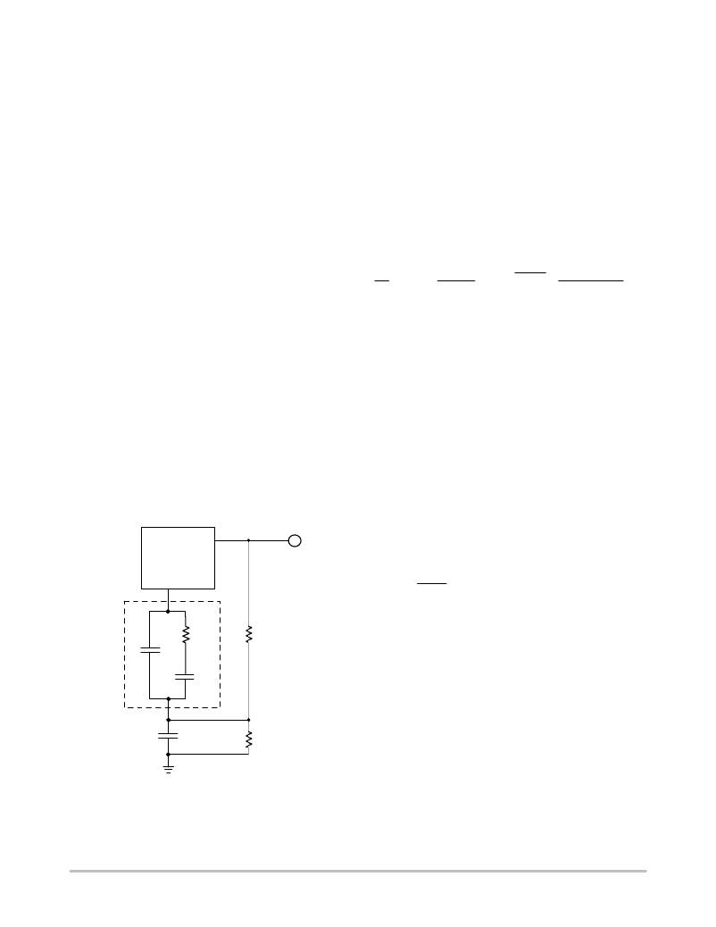
�unwanted� oscillation.� In� that� case,� an� external� circuit,� shown�
�in� Figure� 39,� can� be� added� to� increase� the� amount� of� slope�
�compensation� used.� This� circuit� requires� only� a� few�
�components� and� is� “tacked� on”� to� the� compensation�
�network.�
�V� SW� V� SW�
�V� C�
�The� dashed� box� contains� the� normal� compensation�
�circuitry� to� limit� the� bandwidth� of� the� error� amplifier.�
�Resistors� R2� and� R3� form� a� voltage� divider� off� of� the� V� SW�
�pin.� In� normal� operation,� V� SW� looks� similar� to� a� square�
�wave,� and� is� dependent� on� the� converter� topology.� Formulas�
�for� calculating� V� SW� in� the� boost� and� flyback� topologies� are�
�given� in� the� section� “V� SW� Voltage� Limit.”� The� voltage� on�
�V� SW� charges� capacitor� C3� when� the� switch� is� off,� causing�
�the� voltage� at� the� V� C� pin� to� shift� upwards.� When� the� switch�
�turns� on,� C3� discharges� through� R3,� producing� a� negative�
�slope� at� the� V� C� pin.� This� negative� slope� provides� the� slope�
�compensation.�
�The� amount� of� slope� compensation� added� by� this� circuit�
�is�
�*� (1� *� D)�
�D� T� SW� R� 2� )� R� 3� (1� *� D)REAV�
�where:�
�D� I/� D� T� =� the� amount� of� slope� compensation� added� (A/s);�
�V� SW� =� the� voltage� at� the� switch� node� when� the� transistor�
�is� turned� off� (V);�
�f� SW� =� the� switching� frequency,� typically� 280� kHz�
�(CS5171/3)� or� 560� kHz� (CS5172/4)� (Hz);�
�D� =� the� duty� cycle;�
�R� E� =� 0.063� W� ,� the� value� of� the� internal� emitter� resistor;�
�A� V� =� 5� V/V,� the� gain� of� the� current� sense� amplifier.�
�In� selecting� appropriate� values� for� the� slope� compensation�
�network,� the� designer� is� advised� to� choose� a� convenient�
�capacitor,� then� select� values� for� R2� and� R3� such� that� the�
�amount� of� slope� compensation� added� is� 100� mA/� m� s.� Then�
�R2� may� be� increased� or� decreased� as� necessary.� Of� course,�
�the� series� combination� of� R2� and� R3� should� be� large� enough�
�to� avoid� drawing� excessive� current� from� V� SW� .� Additionally,�
�to� ensure� that� the� control� loop� stability� is� improved� ,� the� time�
�constant� formed� by� the� additional� components� should� be�
�chosen� such� that�
�fSW�
�Finally,� it� is� worth� mentioning� that� the� added� slope�
�compensation� is� a� tradeoff� between� duty� cycle� stability� and�
�C1�
�C3�
�R1�
�C2�
�R2�
�R3�
�transient� response.� The� more� slope� compensation� a� designer�
�adds,� the� slower� the� transient� response� will� be,� due� to� the�
�external� circuitry� interfering� with� the� proper� operation� of� the�
�error� amplifier.�
�Soft� ?� Start�
�Through� the� addition� of� an� external� circuit,� a� Soft� ?� Start�
�function� can� be� added� to� the� CS5171/2/3/4� family� of�
�components.� Soft� ?� Start� circuitry� prevents� the� V� C� pin� from�
�slamming� high� during� startup,� thereby� inhibiting� the�
�inductor� current� from� rising� at� a� high� slope.�
�Figure� 39.� Technique� for� Increasing� Slope�
�Compensation�
�http://onsemi.com�
�15�
�相关PDF资料 |
PDF描述 |
|---|---|
| VI-J6K-EY-F2 | CONVERTER MOD DC/DC 40V 50W |
| ABM10DTBT-S664 | CONN EDGECARD 20POS R/A .156 |
| HBM28DRYI | CONN EDGECARD 56POS DIP .156 SLD |
| XC6217A302MR-G | IC REG LDO 3V .2A SOT-25 |
| EMM28DTMH | CONN EDGECARD 56POS R/A .156 SLD |
相关代理商/技术参数 |
参数描述 |
|---|---|
| CS5172ED8G | 功能描述:直流/直流开关调节器 1.5A High Efficiency Boost RoHS:否 制造商:International Rectifier 最大输入电压:21 V 开关频率:1.5 MHz 输出电压:0.5 V to 0.86 V 输出电流:4 A 输出端数量: 最大工作温度: 安装风格:SMD/SMT 封装 / 箱体:PQFN 4 x 5 |
| CS5172EDR8 | 功能描述:直流/直流开关调节器 1.5A High Efficiency RoHS:否 制造商:International Rectifier 最大输入电压:21 V 开关频率:1.5 MHz 输出电压:0.5 V to 0.86 V 输出电流:4 A 输出端数量: 最大工作温度: 安装风格:SMD/SMT 封装 / 箱体:PQFN 4 x 5 |
| CS5172EDR8G | 功能描述:直流/直流开关调节器 1.5A High Efficiency Boost RoHS:否 制造商:International Rectifier 最大输入电压:21 V 开关频率:1.5 MHz 输出电压:0.5 V to 0.86 V 输出电流:4 A 输出端数量: 最大工作温度: 安装风格:SMD/SMT 封装 / 箱体:PQFN 4 x 5 |
| CS5172GD8 | 功能描述:直流/直流开关调节器 1.5A High Efficiency RoHS:否 制造商:International Rectifier 最大输入电压:21 V 开关频率:1.5 MHz 输出电压:0.5 V to 0.86 V 输出电流:4 A 输出端数量: 最大工作温度: 安装风格:SMD/SMT 封装 / 箱体:PQFN 4 x 5 |
| CS5172GD8G | 功能描述:直流/直流开关调节器 1.5A High Efficiency Boost RoHS:否 制造商:International Rectifier 最大输入电压:21 V 开关频率:1.5 MHz 输出电压:0.5 V to 0.86 V 输出电流:4 A 输出端数量: 最大工作温度: 安装风格:SMD/SMT 封装 / 箱体:PQFN 4 x 5 |
发布紧急采购,3分钟左右您将得到回复。