- 您现在的位置:买卖IC网 > PDF目录19355 > CS8126-1YT5 (ON Semiconductor)IC REG LDO 5V .5A TO220-5 PDF资料下载
参数资料
| 型号: | CS8126-1YT5 |
| 厂商: | ON Semiconductor |
| 文件页数: | 8/9页 |
| 文件大小: | 0K |
| 描述: | IC REG LDO 5V .5A TO220-5 |
| 产品变化通告: | Product Discontinuation 03/Apr/2007 |
| 标准包装: | 50 |
| 稳压器拓扑结构: | 正,固定式 |
| 输出电压: | 5V |
| 输入电压: | 6 V ~ 26 V |
| 电压 - 压降(标准): | 0.35V @ 500mA |
| 稳压器数量: | 1 |
| 电流 - 输出: | 500mA |
| 电流 - 限制(最小): | 750mA |
| 工作温度: | -40°C ~ 125°C |
| 安装类型: | 通孔 |
| 封装/外壳: | TO-220-5 |
| 供应商设备封装: | TO-220-5 |
| 包装: | 管件 |
| 其它名称: | CS8126-1YT5OS |
�� �
�
�CS8126�
�R� Q� JA� +�
�150� °� C� *� TA�
�PD�
�Step� 1:� Place� the� completed� circuit� with� a� tantalum�
�capacitor� of� the� recommended� value� in� an� environmental�
�chamber� at� the� lowest� specified� operating� temperature� and�
�monitor� the� outputs� with� an� oscilloscope.� A� decade� box�
�connected� in� series� with� the� capacitor� will� simulate� the�
�higher� ESR� of� an� aluminum� capacitor.� Leave� the� decade� box�
�outside� the� chamber,� the� small� resistance� added� by� the�
�longer� leads� is� negligible.�
�Step� 2:� With� the� input� voltage� at� its� maximum� value,�
�increase� the� load� current� slowly� from� zero� to� full� load� while�
�observing� the� output� for� any� oscillations.� If� no� oscillations�
�are� observed,� the� capacitor� is� large� enough� to� ensure� a� stable�
�design� under� steady� state� conditions.�
�Step� 3:� Increase� the� ESR� of� the� capacitor� from� zero� using� the�
�decade� box� and� vary� the� load� current� until� oscillations�
�appear.� Record� the� values� of� load� current� and� ESR� that� cause�
�the� greatest� oscillation.� This� represents� the� worst� case� load�
�conditions� for� the� regulator� at� low� temperature.�
�where:�
�V� IN(max)� is� the� maximum� input� voltage,�
�V� OUT(min)� is� the� minimum� output� voltage,�
�I� OUT(max)� is� the� maximum� output� current,� for� the�
�application,� and�
�I� Q� is� the� quiescent� current� the� regulator� consumes� at�
�I� OUT(max)� .�
�Once� the� value� of� P� D(max)� is� known,� the� maximum�
�permissible� value� of� R� q� JA� can� be� calculated:�
�(2)�
�The� value� of� R� q� JA� can� then� be� compared� with� those� in� the�
�package� section� of� the� data� sheet.� Those� packages� with�
�R� q� JA� ’s� less� than� the� calculated� value� in� equation� 2� will� keep�
�the� die� temperature� below� 150� °� C.�
�In� some� cases,� none� of� the� packages� will� be� sufficient� to�
�dissipate� the� heat� generated� by� the� IC,� and� an� external�
�heatsink� will� be� required.�
�Step� 4:� Maintain� the� worst� case� load� conditions� set� in� step�
�3� and� vary� the� input� voltage� until� the� oscillations� increase.�
�This� point� represents� the� worst� case� input� voltage�
�conditions.�
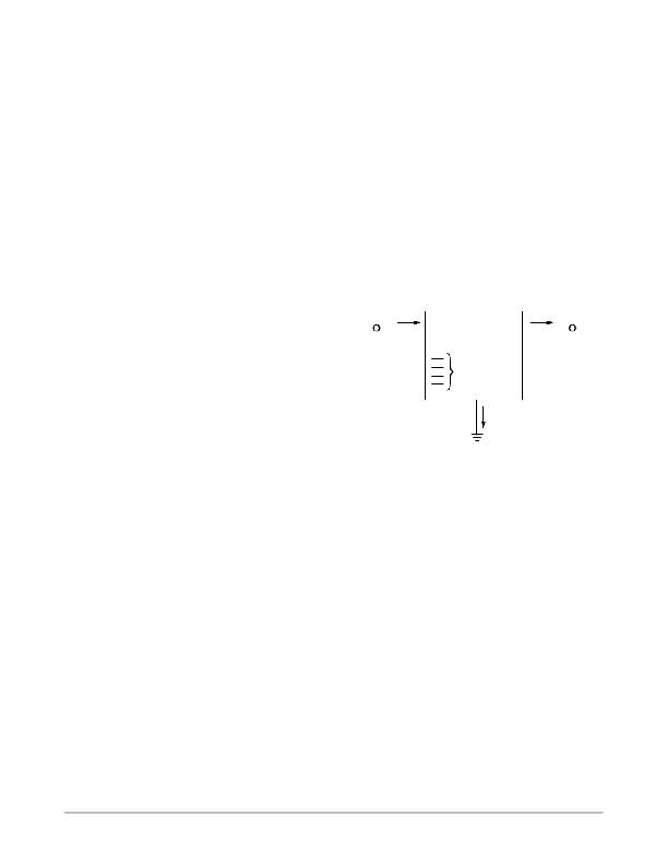
�V� IN�
�I� IN�
�SMART�
�REGULATOR� ?�
�I� OUT�
�V� OUT�
�Step� 5:� If� the� capacitor� is� adequate,� repeat� steps� 3� and� 4� with�
�the� next� smaller� valued� capacitor.� A� smaller� capacitor� will�
�usually� cost� less� and� occupy� less� board� space.� If� the� output�
�oscillates� within� the� range� of� expected� operating� conditions,�
�repeat� steps� 3� and� 4� with� the� next� larger� standard� capacitor�
�value.�
�Step� 6:� Test� the� load� transient� response� by� switching� in�
�various� loads� at� several� frequencies� to� simulate� its� real�
�working� environment.� Vary� the� ESR� to� reduce� ringing.�
�Step� 7:� Raise� the� temperature� to� the� highest� specified�
�operating� temperature.� Vary� the� load� current� as� instructed� in�
�step� 5� to� test� for� any� oscillations.�
�Once� the� minimum� capacitor� value� with� the� maximum�
�ESR� is� found,� a� safety� factor� should� be� added� to� allow� for� the�
�tolerance� of� the� capacitor� and� any� variations� in� regulator�
�performance.� Most� good� quality� aluminum� electrolytic�
�capacitors� have� a� tolerance� of� ±� 20%� so� the� minimum� value�
�found� should� be� increased� by� at� least� 50%� to� allow� for� this�
�tolerance� plus� the� variation� which� will� occur� at� low�
�temperatures.� The� ESR� of� the� capacitor� should� be� less� than�
�50%� of� the� maximum� allowable� ESR� found� in� step� 3� above.�
�Calculating� Power� Dissipation� in� a� Single� Output�
�Linear� Regulator�
�The� maximum� power� dissipation� for� a� single� output�
�regulator� (Figure� 14)� is:�
�PD(max)� +� VIN(max)� *� VOUT(min)� IOUT(max)� )� VIN(max)IQ� (1)�
�Control�
�Features�
�I� Q�
�Figure� 14.� Single� Output� Regulator� With� Key�
�Performance� Parameters� Labeled�
�Heat� Sinks�
�A� heat� sink� effectively� increases� the� surface� area� of� the�
�package� to� improve� the� flow� of� heat� away� from� the� IC� and�
�into� the� surrounding� air.�
�Each� material� in� the� heat� flow� path� between� the� IC� and� the�
�outside� environment� will� have� a� thermal� resistance.� Like�
�series� electrical� resistances,� these� resistances� are� summed� to�
�determine� the� value� of� R� q� JA� .�
�R� Q� JA� +� R� Q� JC� )� R� Q� CS� )� R� Q� SA� (3)�
�where:�
�R� q� JC� =� the� junction� ?� to� ?� case� thermal� resistance,�
�R� q� CS� =� the� case� ?� to� ?� heatsink� thermal� resistance,� and�
�R� q� SA� =� the� heatsink� ?� to� ?� ambient� thermal� resistance.�
�R� q� JC� appears� in� the� package� section� of� the� data� sheet.� Like�
�R� q� JA� ,� it� is� a� function� of� package� type.� R� q� CS� and� R� q� SA� are�
�functions� of� the� package� type,� heatsink� and� the� interface�
�between� them.� These� values� appear� in� heat� sink� data� sheets�
�of� heat� sink� manufacturers.�
�http://onsemi.com�
�8�
�相关PDF资料 |
PDF描述 |
|---|---|
| MSC7119VF1200 | DSP 16BIT W/DDR CTRLR 400-MAPBGA |
| HWS600-48 | PWR SUP IND 48V 13A SNG OUTPUT |
| MAX6581TG9C+ | IC TEMP SENSOR 8-CH PREC 24-TQFN |
| ATFC-0402-1N9-BT | INDUCTOR THIN FILM 1.9NH 0402 |
| VE-BTL-CV-F3 | CONVERTER MOD DC/DC 28V 150W |
相关代理商/技术参数 |
参数描述 |
|---|---|
| CS8126-1YT5G | 功能描述:低压差稳压器 - LDO ANA 5V 750MA LIN RoHS:否 制造商:Texas Instruments 最大输入电压:36 V 输出电压:1.4 V to 20.5 V 回动电压(最大值):307 mV 输出电流:1 A 负载调节:0.3 % 输出端数量: 输出类型:Fixed 最大工作温度:+ 125 C 安装风格:SMD/SMT 封装 / 箱体:VQFN-20 |
| CS8126-1YTHA5 | 功能描述:低压差稳压器 - LDO 5V 750mA RoHS:否 制造商:Texas Instruments 最大输入电压:36 V 输出电压:1.4 V to 20.5 V 回动电压(最大值):307 mV 输出电流:1 A 负载调节:0.3 % 输出端数量: 输出类型:Fixed 最大工作温度:+ 125 C 安装风格:SMD/SMT 封装 / 箱体:VQFN-20 |
| CS8126-1YTHA5G | 功能描述:低压差稳压器 - LDO ANA 5V 750MA LIN RoHS:否 制造商:Texas Instruments 最大输入电压:36 V 输出电压:1.4 V to 20.5 V 回动电压(最大值):307 mV 输出电流:1 A 负载调节:0.3 % 输出端数量: 输出类型:Fixed 最大工作温度:+ 125 C 安装风格:SMD/SMT 封装 / 箱体:VQFN-20 |
| CS8126-1YTHE5 | 功能描述:低压差稳压器 - LDO 5V 750mA RoHS:否 制造商:Texas Instruments 最大输入电压:36 V 输出电压:1.4 V to 20.5 V 回动电压(最大值):307 mV 输出电流:1 A 负载调节:0.3 % 输出端数量: 输出类型:Fixed 最大工作温度:+ 125 C 安装风格:SMD/SMT 封装 / 箱体:VQFN-20 |
| CS8126-1YTHE5G | 功能描述:低压差稳压器 - LDO 5V 750mA w/Delayed Reset RoHS:否 制造商:Texas Instruments 最大输入电压:36 V 输出电压:1.4 V to 20.5 V 回动电压(最大值):307 mV 输出电流:1 A 负载调节:0.3 % 输出端数量: 输出类型:Fixed 最大工作温度:+ 125 C 安装风格:SMD/SMT 封装 / 箱体:VQFN-20 |
发布紧急采购,3分钟左右您将得到回复。