参数资料
| 型号: | CS8190ENF16 |
| 厂商: | ON Semiconductor |
| 文件页数: | 10/11页 |
| 文件大小: | 0K |
| 描述: | IC DRVR AIRCORE TACH/SPEED 16DIP |
| 产品变化通告: | Product Discontinuation 20/Aug/2008 |
| 标准包装: | 25 |
| 类型: | 驱动器 |
| 应用: | 自动 |
| 安装类型: | 通孔 |
| 封装/外壳: | 16-DIP(0.300",7.62mm) |
| 供应商设备封装: | 16-DIP |
| 包装: | 管件 |
| 其它名称: | CS8190ENF16OS |
CS8190
http://onsemi.com
8
R3
R4
R2
C3
C1
D2
R1
D1
GND
COSINE
SINE
C4
CCP
RT
+
Speedo Input
Battery
Air Core
Gauge
200 W
CP+
CP
SQOUT
F/VOUT
VREG
GND
SINE+
SINE
BIAS
FREQIN
GND
COS+
COS
VCC
1
Speedometer
CS8190
Trim Resistor
± 20 PPM/°C
0.1 mF
1.0 A
600 PIV
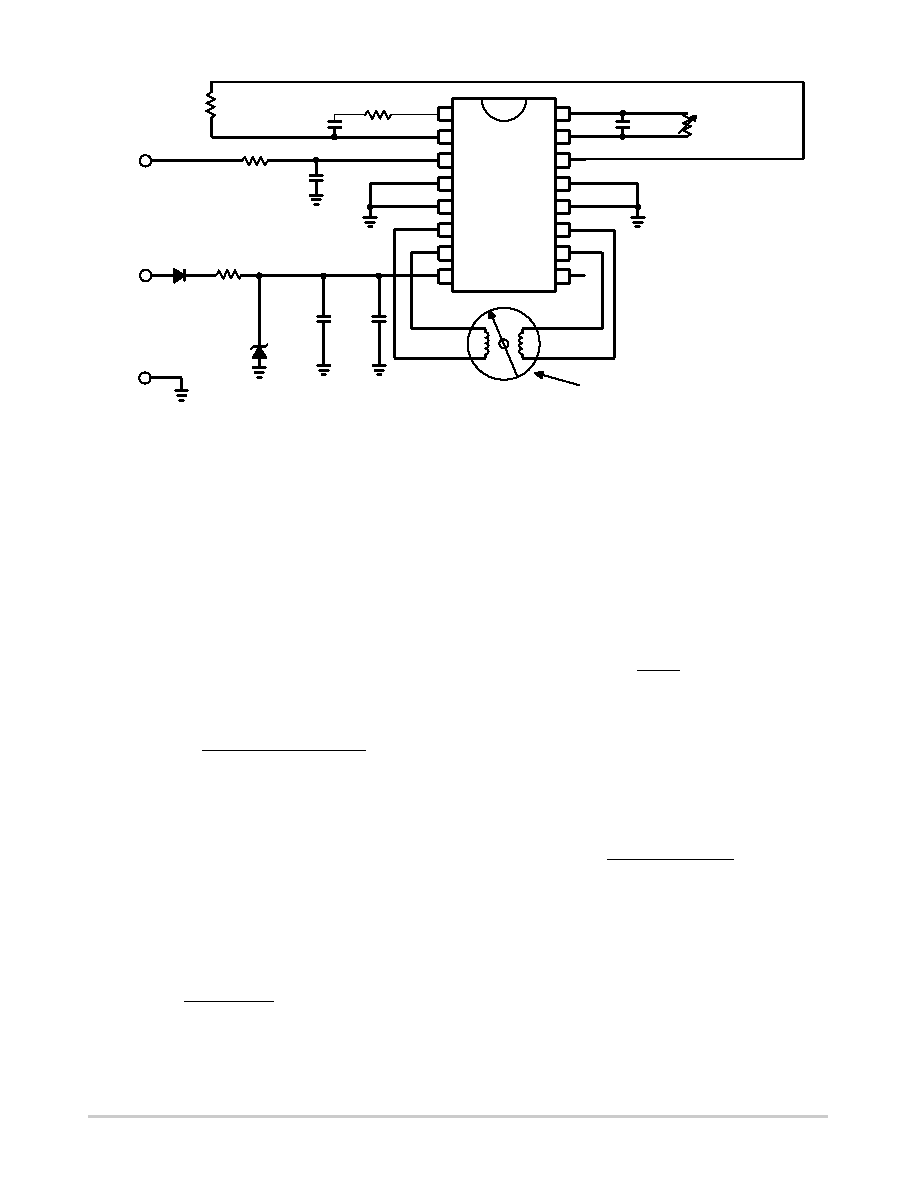
Figure 9. Speedometer or Tachometer Application
3.9,
500 mW
10 kW
3.0 kW
1.0 kW
0.0033 mF
0.47 mF
0.1 mF
50 V,
500 mW
Zener
± 30 PPM/°C
C2
2000 mF
Notes:
1. C2 (> 2000 mF) is needed if return to zero function is required.
2. The product of C4 and RT have a direct effect on gain and therefore directly affect temperature compensation.
3. C4 Range; 20 pF to 0.2 mF.
4. RT Range; 100 kW to 500 kW.
5. The IC must be protected from transients above 60 V and reverse battery conditions.
6. Additional filtering on the FREQIN lead may be required.
7. Gauge coil connections to the IC must be kept as short as possible (≤ 3.0 inch) for best pointer stability.
Design Example
Maximum meter Deflection = 270
°
Maximum Input Frequency = 350 Hz
1. Select RT and CCP
q + 970
FREQ
CCP
RT + 270°
Let CCP = 0.0033 mF, find RT
RT +
270°
970
350 Hz
0.0033 mF
RT + 243 kW
RT should be a 250 k
W potentiometer to trim out any
inaccuracies due to IC tolerances or meter movement
pointer placement.
2. Select R3 and R4
Resistor R3 sets the output current from the voltage
regulator. The maximum output current from the voltage
regulator is 10 mA. R3 must ensure that the current does not
exceed this limit.
Choose R3 = 3.3 k
W
The charge current for CCP is
VREG * 0.7 V
3.3 kW
+ 1.90 mA
CCP must charge and discharge fully during each cycle of
the input signal. Time for one cycle at maximum frequency
is 2.85 ms. To ensure that CCP is charged, assume that the
(R3 + R4) CCP time constant is less than 10% of the
minimum input period.
T + 10%
1
350 Hz +
285 ms
Choose R4 = 1.0 k
W.
Discharge time: tDCHG = R3 × CCP = 3.3 kW × 0.0033 mF
= 10.9
ms
Charge time: tCHG = (R3 + R4)CCP = 4.3 kW. × 0.0033 mF
= 14.2
ms
3. Determine C4
C4 is selected to satisfy both the maximum allowable
ripple voltage and response time of the meter movement.
C4 +
CCP(VREG * 0.7 V)
DVMAX
With C4 = 0.47
mF, the F/V ripple voltage is 44 mV.
The last component to be selected is the return to zero
capacitor C2. This is selected by increasing the input signal
frequency to its maximum so the pointer is at its maximum
deflection, then removing the power from the circuit. C2
should be large enough to ensure that the pointer always
returns to the 0
° position rather than 360° under all operating
conditions.
Figure 10 shows how the CS8190 and the CS8441 are
used to produce a Speedometer and Odometer circuit.
相关PDF资料 |
PDF描述 |
|---|---|
| MIC5333-NNYMT TR | IC REG LDO 2.85V .3A 10TMLF |
| MAX9949DCCB+TD | IC PMU DUAL 64TQFP |
| KS8993MI | IC SWITCH 10/100 3PORT 128PQFP |
| ABM40DTAS | CONN EDGECARD 80POS R/A .156 SLD |
| AMM24DRSS | CONN EDGECARD 48POS DIP .156 SLD |
相关代理商/技术参数 |
参数描述 |
|---|---|
| CS8190ENF16G | 功能描述:马达/运动/点火控制器和驱动器 ANA AIRCORE TACH/ SPEED RoHS:否 制造商:STMicroelectronics 产品:Stepper Motor Controllers / Drivers 类型:2 Phase Stepper Motor Driver 工作电源电压:8 V to 45 V 电源电流:0.5 mA 工作温度:- 25 C to + 125 C 安装风格:SMD/SMT 封装 / 箱体:HTSSOP-28 封装:Tube |
| CS-8190N16 | 制造商:未知厂家 制造商全称:未知厂家 功能描述:Tachometer Circuit |
| CS8191 | 制造商:ONSEMI 制造商全称:ON Semiconductor 功能描述:Precision Air-Core Tach/Speedo Driver |
| CS8191/D | 制造商:ONSEMI 制造商全称:ON Semiconductor 功能描述:Precision Air-Core Tach/Speedo Driverwith Short Circuit Protection |
| CS-8191DW20 | 制造商:未知厂家 制造商全称:未知厂家 功能描述:Meter Driver |
发布紧急采购,3分钟左右您将得到回复。