参数资料
| 型号: | CS8191XNF16 |
| 厂商: | ON Semiconductor |
| 文件页数: | 6/12页 |
| 文件大小: | 0K |
| 描述: | IC DRVR AIRCORE TACH/SPEED 16DIP |
| 产品变化通告: | Product Obsolescence 30/Dec/2003 |
| 标准包装: | 25 |
| 类型: | 驱动器 |
| 电源电压: | 8.5 V ~ 15 V |
| 安装类型: | 通孔 |
| 封装/外壳: | 16-DIP(0.300",7.62mm) |
| 供应商设备封装: | 16-DIP |
| 包装: | 管件 |
| 其它名称: | CS8191XNF16OS |
CS8191
http://onsemi.com
3
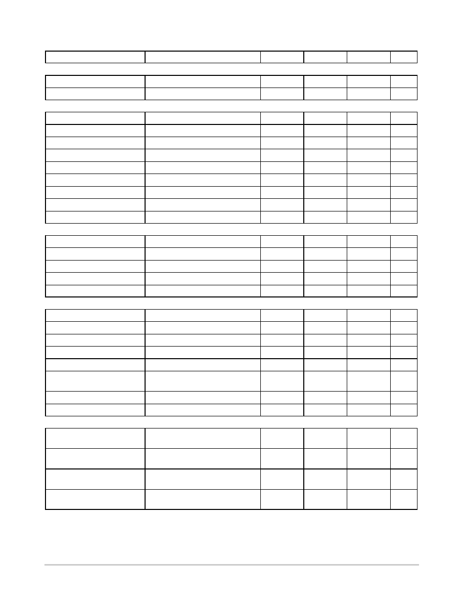
ELECTRICAL CHARACTERISTICS (–40
°C ≤ TA ≤ 105°C, 8.0 V ≤ VCC ≤ 16 V, unless otherwise specified.)
Characteristic
Test Conditions
Min
Typ
Max
Unit
Supply Voltage Section
ICC Supply Current
VCC = 16 V, –40°C, No Load
–
70
125
mA
VCC Normal Operation Range
–
8.0
13.1
16
V
Input Comparator Section
Positive Input Threshold
–
2.4
2.7
3.0
V
Negative Input Threshold
–
2.0
2.3
–
V
Input Hysteresis
–
200
400
1000
mV
Input Bias Current (Note 3.)
0 V
≤ VIN ≤ 8.0 V
–
–2.0
±10
A
Input Frequency Range
–
0
–
20
kHz
Input Voltage Range
in series with 1.0 k
–1.0
–
VCC
V
Output VSAT
ICC = 10 mA
–
0.15
0.40
V
Output Leakage
VCC = 7.0 V
–
10
A
Logic 0 Input Voltage
–
2.0
–
V
Voltage Regulator Section
Output Voltage
–
6.50
7.00
7.50
V
Output Load Current
–
10
mA
Output Load Regulation
0 to 10 mA
–
10
50
mV
Output Line Regulation
8.0 V
≤ VCC ≤ 16 V
–
20
150
mV
Power Supply Rejection
VCC = 13.1 V, 1.0 VP/P 1.0 kHz
34
46
–
dB
Charge Pump Section
Inverting Input Voltage
–
1.5
2.0
2.5
V
Input Bias Current
–
40
150
nA
VBIAS Input Voltage
–
1.5
2.0
2.5
V
Non Invert. Input Voltage
IIN = 1.0 mA
–
0.7
1.1
V
Linearity (Note 4.)
@ 0, 87.5, 175, 262.5, + 350 Hz
–0.10
0.28
+0.70
%
F/VOUT Gain
@ 350 Hz, CCP = 0.0033 F,
RT = 243 k
7.0
10
13
mV/Hz
Norton Gain, Positive
IIN = 15 A
0.9
1.0
1.1
I/I
Norton Gain, Negative
IIN = 15 A
0.9
1.0
1.1
I/I
Function Generator Section: –40
5C 3 TA 3 85°C, VCC = 13.1 V unless otherwise noted.
Differential Drive Voltage
(VCOS+ – VCOS–)
10 V
≤ VCC ≤ 16 V
Θ = 0°
7.5
8.0
8.5
V
Differential Drive Voltage
(VSIN+ – VSIN–)
10 V
≤ VCC ≤ 16 V
Θ = 90°
7.5
8.0
8.5
V
Differential Drive Voltage
(VCOS+ – VCOS–)
10 V
≤ VCC ≤ 16 V
Θ = 180°
–8.5
–8.0
–7.5
V
Differential Drive Voltage
(VSIN+ – VSIN–)
10 V
≤ VCC ≤ 16 V
Θ = 270°
–8.5
–8.0
–7.5
V
3. Input is clamped by an internal 12 V Zener.
4. Applies to % of full scale (270
°).
相关PDF资料 |
PDF描述 |
|---|---|
| CS82C5296 | IC UART/BRG 5V 16MHZ 28-PLCC |
| CS82C59A-1296 | IC CTRL INTERRUPT 12.5MHZ 28PLCC |
| CS8900A-IQZ | IC LAN ETHERNET CTLR 5V 100LQFP |
| CS8952-IQZ | IC TXRX 100/10 PHY 100TQFP |
| CY8CLED04DOCD1-56LTXI | IC POWERPSOC DEBUG 4CH 1A 56VQFN |
相关代理商/技术参数 |
参数描述 |
|---|---|
| CS81GE11PF | 制造商:未知厂家 制造商全称:未知厂家 功能描述:LIGHT-DEPENDENT-RESISTOR-OUTPUT OPTOCOUPLER |
| CS81GE12PF | 制造商:未知厂家 制造商全称:未知厂家 功能描述:Optoelectronic |
| CS81GS52PF | 制造商:未知厂家 制造商全称:未知厂家 功能描述:LIGHT-DEPENDENT-RESISTOR-OUTPUT OPTOCOUPLER |
| CS81W64 | 制造商:Molex 功能描述: |
| CS81W65 | 制造商:Molex 功能描述: 制造商:Woodhead Molex 功能描述: |
发布紧急采购,3分钟左右您将得到回复。