- 您现在的位置:买卖IC网 > PDF目录380119 > CY22391 (Cypress Semiconductor Corp.) Factory Programmable Quad PLL Clock Generator with VCXO(带VCXO的可编程方形PLL时钟发生器) PDF资料下载
参数资料
| 型号: | CY22391 |
| 厂商: | Cypress Semiconductor Corp. |
| 英文描述: | Factory Programmable Quad PLL Clock Generator with VCXO(带VCXO的可编程方形PLL时钟发生器) |
| 中文描述: | 四工厂可编程锁相环时钟发生器,石英振荡器(带石英振荡器的可编程方形锁相环时钟发生器) |
| 文件页数: | 2/10页 |
| 文件大小: | 552K |
| 代理商: | CY22391 |
CY22388/89/91
Document #: 38-07734 Rev. *B
Page 2 of 10
General Description
The CY22388 family of devices has an Analog VCXO (Voltage
Controlled Crystal Oscillator), 4 PLLs, up to 8 clock outputs
and frequency selection capabilities. The frequency selects do
not modify any PLL frequency. Instead they allow the user to
choose between up to 8 different output divider selections
depending on the clock and package configuration. This is
illustrated in the following Frequency Selection tables and
Functional Block Diagram.
There is one programmable OE/PDWN. The OE/PDWN pin
can be programmed as either an output enable pin or a
power-down pin. The OE function can be programmed to
disable a selected set of outputs when low, leaving the
remaining outputs running. Full-chip power down will disable
all outputs as well as the PLLs and most of the active circuitry
when low.
Factory-Programmable CY22388/89/91
Factory programming is available for high- or low-volume
manufacturing by Cypress. All requests must be submitted to
the local Cypress Field Application Engineer (FAE) or sales
representative. Once therequest has beenprocessed, you will
receive a new part number, samples, and data sheet with the
programmed values. This part number will be used for
additional sample requests and production orders.
PLLs
The advantage of having four PLLs is that a single device can
generate up to four independent frequencies from a single
crystal. Generally a design may require up to four oscillators
to accomplish what could be done with a single CY22388.
Each PLL is independent and can be configured to generate
a VCO (Voltage Controlled Oscillator) frequency between
62.5 MHz and 250 MHz. Each PLL can then in turn be divided
down with post dividers to generate the clock output frequency
of the user’s choice. The output divider allows each clock
output to be divided by 1,2,3,4,5,6,8,9,10,12,15. The PLL
maximum is reduced to 166 MHz in divide by 1 mode due to
output buffer limitations.
Outputs that allow frequency switching perform the transition
free of glitches. A glitch is defined as a high or low time shorter
than half the smaller of the two periods being switched
between. Extended low time (even many cycles in duration) is
acceptable.
Selected clock outputs are capable of being powered off a
separate 2.5V supply. This will allow for driving lower voltage
swing inputs. The CY22388/89/91 device still requires 3.3V to
power the oscillator and all other internal PLL circuitry. For the
2.5V output option please refer to the CY22388 Application
Note. Selected clocks and pinout diagrams will be explained
in this application note.
Clock D can obtain its output from either the reference source
or PLL1/N1 with N1 being defined as the output divider for
PLL1. Clock H is defined as a copy of clock D. Clock D is only
available from PLL1/N1 on the 16-pin package.
For CY22388, CLKB and CLKC have related frequencies. For
CY22389 and CY22391, CLKD and CLKF have related
frequencies, CLKA and CLKB have related frequencies, and
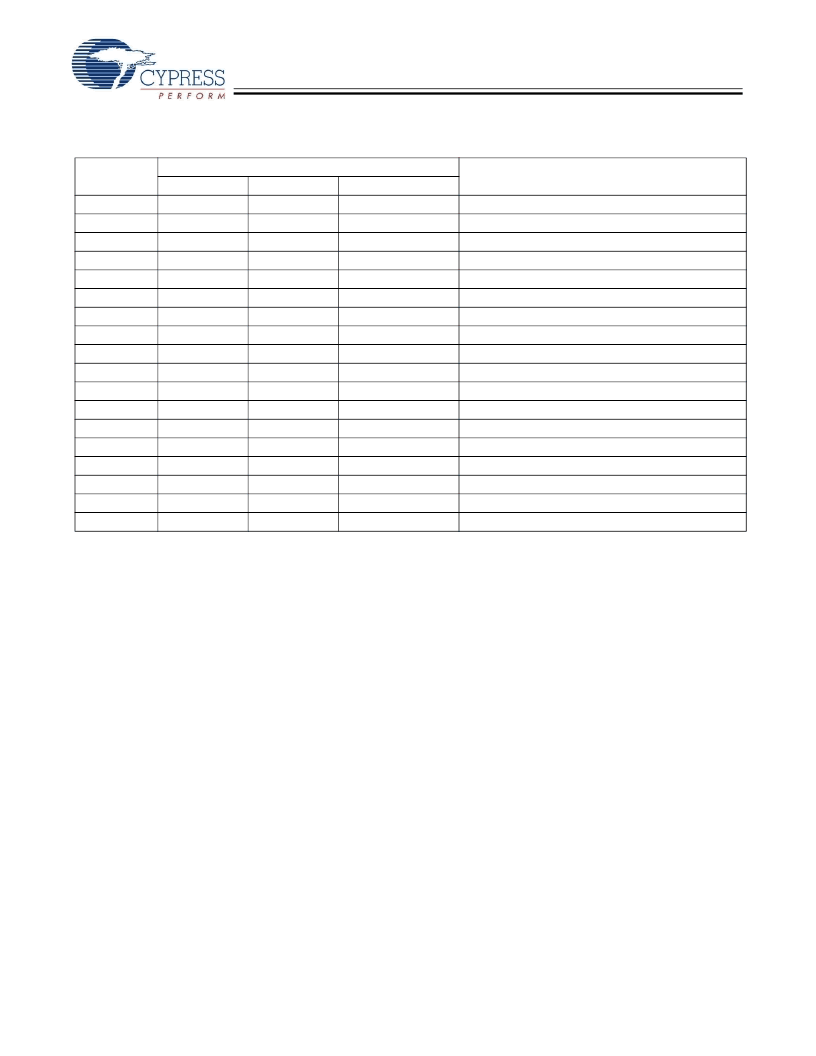
Pin Description
Pin Name
Pin Number
Pin Description
16-Pin TSSOP 20-Pin TSSOP
1
16
7
8
9
10
11
n/a
n/a
n/a
2
3
14
n/a
4
5,13,15
6,12
n/a
32-Pin QFN
30
27
11
10
14
9
15
17
18
8
31
32
23
24
1
2,3,16,21,22,25,26
4,5,6,7,19,20
12,13,28,29
XIN
XOUT
CLKA
CLKB
CLKC
CLKD
CLKE
CLKF
CLKG
CLKH
FS0
FS1
FS2
OE/PD
VIN
VDD
VSS
NC
1
Crystal Input or Reference Clock Input
Crystal Output (No connect if external clock is used)
Clock Output
Clock Output
Clock Output
Clock Output
Clock Output
Clock Output
Clock Output
Clock Output
Frequency Select 0
Frequency Select 1
Frequency Select 2
Output Enable Control/Power Down
Analog Control Input for VCXO
Voltage Supply
Ground
No Connect.
20
9
8
10
7
11
12
13
4
2
3
17
18
16
5,15,19
6,14
n/a
相关PDF资料 |
PDF描述 |
|---|---|
| CY22392 | Three-PLL General Purpose FLASH Programmable Clock Generator(通用三锁相环FLASH可编程时钟发生器) |
| CY22393 | -bit AVR Microcontroller with 8K Bytes In- System Programmable Flash |
| CY22394 | -bit AVR Microcontroller with 8K Bytes In- System Programmable Flash |
| CY2254A | Pentium Processor Compatible Clock Synthesizer/Driver(奔腾处理器兼容的时钟合成器/驱动器) |
| CY2254 | Two-PLL Clock Generator(二锁相环时钟发生器) |
相关代理商/技术参数 |
参数描述 |
|---|---|
| CY22391KLTFXC | 制造商:Cypress Semiconductor 功能描述: |
| CY22391KLTXC-01 | 功能描述:时钟发生器及支持产品 Factory Program Quad PLL Clk Gen w/VCXO RoHS:否 制造商:Silicon Labs 类型:Clock Generators 最大输入频率:14.318 MHz 最大输出频率:166 MHz 输出端数量:16 占空比 - 最大:55 % 工作电源电压:3.3 V 工作电源电流:1 mA 最大工作温度:+ 85 C 安装风格:SMD/SMT 封装 / 箱体:QFN-56 |
| CY22391KLTXC-01KG | 制造商:Cypress Semiconductor 功能描述: |
| CY22391KLTXC-01T | 功能描述:时钟发生器及支持产品 Factory Program Quad PLL Clk Gen w/VCXO RoHS:否 制造商:Silicon Labs 类型:Clock Generators 最大输入频率:14.318 MHz 最大输出频率:166 MHz 输出端数量:16 占空比 - 最大:55 % 工作电源电压:3.3 V 工作电源电流:1 mA 最大工作温度:+ 85 C 安装风格:SMD/SMT 封装 / 箱体:QFN-56 |
| CY22391KLTXC-02 | 功能描述:时钟发生器及支持产品 Factory Program Quad PLL Clk Gen w/VCXO RoHS:否 制造商:Silicon Labs 类型:Clock Generators 最大输入频率:14.318 MHz 最大输出频率:166 MHz 输出端数量:16 占空比 - 最大:55 % 工作电源电压:3.3 V 工作电源电流:1 mA 最大工作温度:+ 85 C 安装风格:SMD/SMT 封装 / 箱体:QFN-56 |
发布紧急采购,3分钟左右您将得到回复。