- 您现在的位置:买卖IC网 > PDF目录9606 > CY28411ZXCT (Silicon Laboratories Inc)IC CLOCK CK410M ALVISO 56TSSOP PDF资料下载
参数资料
| 型号: | CY28411ZXCT |
| 厂商: | Silicon Laboratories Inc |
| 文件页数: | 12/18页 |
| 文件大小: | 0K |
| 描述: | IC CLOCK CK410M ALVISO 56TSSOP |
| 标准包装: | 2,000 |
| 类型: | 时钟/频率发生器 |
| PLL: | 是 |
| 主要目的: | Intel CPU 服务器 |
| 输入: | LVTTL,晶体 |
| 输出: | HCSL,LVCMOS |
| 电路数: | 1 |
| 比率 - 输入:输出: | 3:19 |
| 差分 - 输入:输出: | 无/是 |
| 频率 - 最大: | 133MHz |
| 电源电压: | 3.135 V ~ 3.465 V |
| 工作温度: | 0°C ~ 85°C |
| 安装类型: | 表面贴装 |
| 封装/外壳: | 56-TFSOP(0.240",6.10mm 宽) |
| 供应商设备封装: | 56-TSSOP |
| 包装: | 带卷 (TR) |
| 其它名称: | SLCY28411ZXCT |
CY28411
........................ Document #: 38-07594 Rev. *B Page 3 of 18
Frequency Select Pins (FS_A, FS_B and FS_C)
Host clock frequency selection is achieved by applying the
appropriate logic levels to FS_A, FS_B, FS_C inputs prior to
VTT_PWRGD# assertion (as seen by the clock synthesizer).
Upon VTT_PWRGD# being sampled low by the clock chip
(indicating processor VTT voltage is stable), the clock chip
samples the FS_A, FS_B and FS_C input values. For all logic
levels of FS_A, FS_B and FS_C, VTT_PWRGD# employs a
one-shot
functionality
in
that
once
a
valid
low
on
VTT_PWRGD# has been sampled, all further VTT_PWRGD#,
FS_A, FS_B and FS_C transitions will be ignored, except in
test mode.
Serial Data Interface
To enhance the flexibility and function of the clock synthesizer,
a two-signal serial interface is provided. Through the Serial
Data Interface, various device functions, such as individual
clock output buffers, can be individually enabled or disabled.
The registers associated with the Serial Data Interface
initializes to their default setting upon power-up, and therefore
use of this interface is optional. Clock device register changes
are normally made upon system initialization, if any are
required. The interface cannot be used during system
operation for power management functions.
Data Protocol
The clock driver serial protocol accepts byte write, byte read,
block write, and block read operations from the controller. For
block write/read operation, the bytes must be accessed in
sequential order from lowest to highest byte (most significant
bit first) with the ability to stop after any complete byte has
been transferred. For byte write and byte read operations, the
system controller can access individually indexed bytes. The
offset of the indexed byte is encoded in the command code,
as described in Table 2.
The block write and block read protocol is outlined in Table 3
while Table 4 outlines the corresponding byte write and byte
read protocol. The slave receiver address is 11010010 (D2h).
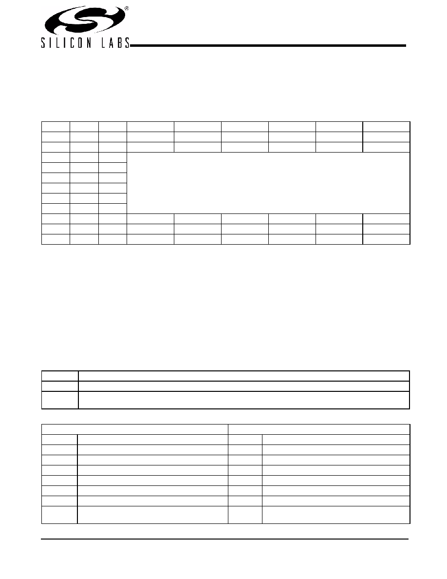
Table 1. Frequency Select Table FS_A, FS_B and FS_C
FS_C
FS_B
FS_A
CPU
SRC
PCIF/PCI
REF0
DOT96
USB
MID
0
1
100 MHz
33 MHz
14.318 MHz
96 MHz
48 MHz
0
1
133 MHz
100 MHz
33 MHz
14.318 MHz
96 MHz
48 MHz
011
RESERVED
010
000
MID
0
MID
1
0
MID
1
0
x
Hi-Z
1
0
REF/2
REF/8
REF/24
REF
1
REF/2
REF/8
REF/24
REF
Table 2. Command Code Definition
Bit
Description
7
0 = Block read or block write operation, 1 = Byte read or byte write operation
(6:0)
Byte offset for byte read or byte write operation. For block read or block write operations, these bits should be
'0000000'
Table 3. Block Read and Block Write Protocol
Block Write Protocol
Block Read Protocol
Bit
Description
Bit
Description
1Start
1
Start
8:2
Slave address – 7 bits
8:2
Slave address – 7 bits
9
Write
9
Write
10
Acknowledge from slave
10
Acknowledge from slave
18:11
Command Code – 8 bits
18:11
Command Code – 8 bits
19
Acknowledge from slave
19
Acknowledge from slave
27:20
Byte Count – 8 bits
(Skip this step if I2C_EN bit set)
20
Repeat start
相关PDF资料 |
PDF描述 |
|---|---|
| ICL3232EIV-16T | IC 2DRVR/2RCVR RS232 3V 16-TSSOP |
| VE-2WT-MX-F4 | CONVERTER MOD DC/DC 6.5V 75W |
| V375B2H100BL2 | CONVERTER MOD DC/DC 2V 100W |
| D38999/20FJ29SB | CONN RCPT 29POS WALL MNT W/SCKT |
| VE-2WT-MX-F1 | CONVERTER MOD DC/DC 6.5V 75W |
相关代理商/技术参数 |
参数描述 |
|---|---|
| CY28411ZXCT-1 | 制造商:CYPRESS 制造商全称:Cypress Semiconductor 功能描述:Clock Generator for Intel Alviso Chipset |
| CY28412 | 制造商:SPECTRALINEAR 制造商全称:SPECTRALINEAR 功能描述:Clock Generator for Intel㈢ Grantsdale Chipset |
| CY28412OC | 制造商:SPECTRALINEAR 制造商全称:SPECTRALINEAR 功能描述:Clock Generator for Intel㈢ Grantsdale Chipset |
| CY28412OCT | 制造商:SPECTRALINEAR 制造商全称:SPECTRALINEAR 功能描述:Clock Generator for Intel㈢ Grantsdale Chipset |
| CY28412OXC | 功能描述:IC CLOCK GEN GRANTSDALE 56-SSOP RoHS:是 类别:集成电路 (IC) >> 时钟/计时 - 专用 系列:- 标准包装:1,500 系列:- 类型:时钟缓冲器/驱动器 PLL:是 主要目的:- 输入:- 输出:- 电路数:- 比率 - 输入:输出:- 差分 - 输入:输出:- 频率 - 最大:- 电源电压:3.3V 工作温度:0°C ~ 70°C 安装类型:表面贴装 封装/外壳:28-SSOP(0.209",5.30mm 宽) 供应商设备封装:28-SSOP 包装:带卷 (TR) 其它名称:93786AFT |
发布紧急采购,3分钟左右您将得到回复。