- 您现在的位置:买卖IC网 > PDF目录2067 > CY28508OXC (Silicon Laboratories Inc)IC CLOCK SSCG 3DIFF PAIR 28SSOP PDF资料下载
参数资料
| 型号: | CY28508OXC |
| 厂商: | Silicon Laboratories Inc |
| 文件页数: | 8/13页 |
| 文件大小: | 0K |
| 描述: | IC CLOCK SSCG 3DIFF PAIR 28SSOP |
| 标准包装: | 47 |
| 类型: | * |
| PLL: | 是 |
| 输入: | 晶体 |
| 输出: | 时钟 |
| 电路数: | 1 |
| 比率 - 输入:输出: | 1:4 |
| 差分 - 输入:输出: | 无/是 |
| 频率 - 最大: | 333.3MHz |
| 除法器/乘法器: | 是/无 |
| 电源电压: | 2.375 V ~ 3.465 V |
| 工作温度: | 0°C ~ 70°C |
| 安装类型: | * |
| 封装/外壳: | * |
| 供应商设备封装: | * |
| 包装: | * |
CY28508
........................ Document #: 38-07534 Rev. *F Page 4 of 13
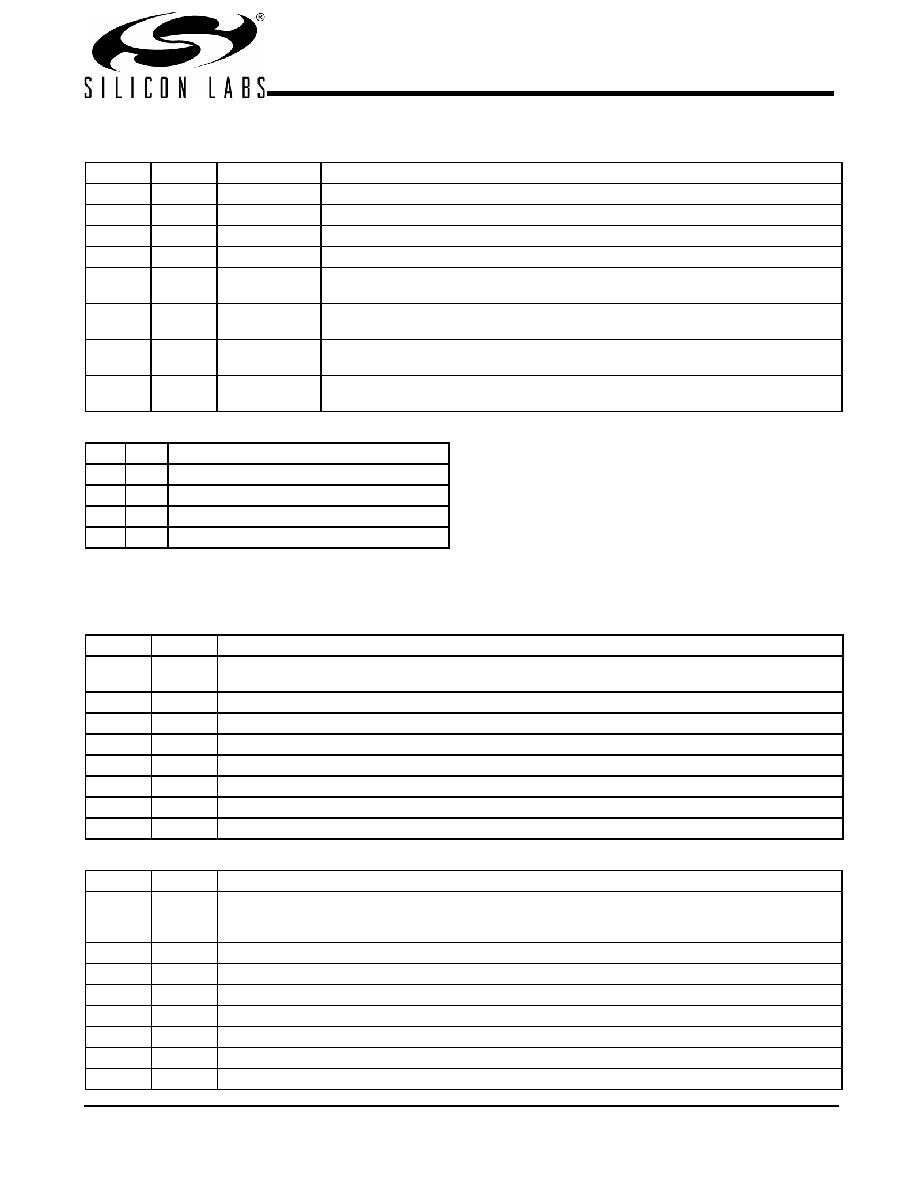
Serial Control Registers
Glitch-free operation for both enabling and disabling Spread
Spectrum. To achieve down spread operation, reprogram the
N register to drop the frequency by half the spread amount.
Byte 0 : CPU Control Register
Bit
@Pup
Name
Description
7
HW
LOCK
Lock Detect: 0 = not at final frequency, 1 = VCO locked (read-only).
6
0
SS_ENABLE
0 = disabled, 1 = enabled.
5
0
SST1
Select spread percentage 1. See Table 4
4
1
SST0
Select spread percentage 0. See Table 4
3
1
REF
REF Output Enable
0 = Disabled (three-stated)), 1 = Enabled
2
1
CPUT/C2
CPU2 Output Enable
0 = Disabled (three-stated), 1 = Enabled
1
CPUT/C1
CPU1 Output Enable
0 = Disabled (three-stated), 1 = Enabled
0
1
CPUT/C0
CPU0 Output Enable
0 = Disabled (three-stated), 1 = Enabled
Table 4. Spread Spectrum Table
SST1 SST0
% Spread
00
0.125% Center spread Lexmark profile
01
0.25% Center spread Lexmark profile
10
0.5% Center spread Lexmark profile
11
0.5% Center spread Linear profile
Byte 1: Dial-a-Frequency Control Register N0 [default = 112.35 MHz, N = 43d, ODSEL = 1]
Bit
@Pup
Description
7
0
Test Mode: 0 = normal operation, 1 = phase-locked loop (PLL) bypass mode, when OD = 3 then /3, when
OD = 2 then /2.
6
0
N6, most significant bit (MSB).
51
N5
40
N4
31
N3
20
N2
11
N1
0
1
N0, least significant bit (LSB).
Byte 2: Dial-a-Frequency Control Register M0 [default = 112.35MHz, M = 49d, ODSEL = 1]
Bit
@Pup
Description
7
0
The charge pump current value during Smooth-Track can be programmed to normal mode (2xICP) by
setting this bit to “1.” The default value of “0” (1xICP) will program the charge pump current to half of normal
and will reduce the bandwidth and hence the slew rate.
6
Pin 6
FSEL operational status, whether HW or SW. 0 = M&N0, 1 = M&N1 (read only).
5
1
M5 MSB
41
M4
30
M3
20
M2
10
M1
01
M0, LSB
相关PDF资料 |
PDF描述 |
|---|---|
| CY2SSTV850ZI | IC CLOCK DIFFDRV PLL DDR 48TSSOP |
| D2-24044-MR | IC DGTL AMP AUDIO PWR D 38HTSSOP |
| D2-45157-QR | IC DGTL AMP PWM CTRLR 68QFN |
| DS1080CLU+ | IC CRYSTAL MULTIPLIER SS 8-MSOP |
| DS1080LU+A00 | IC CRYSTAL MULT SS 8-USOP |
相关代理商/技术参数 |
参数描述 |
|---|---|
| CY28508OXCT | 功能描述:时钟发生器及支持产品 Power PC RoHS:否 制造商:Silicon Labs 类型:Clock Generators 最大输入频率:14.318 MHz 最大输出频率:166 MHz 输出端数量:16 占空比 - 最大:55 % 工作电源电压:3.3 V 工作电源电流:1 mA 最大工作温度:+ 85 C 安装风格:SMD/SMT 封装 / 箱体:QFN-56 |
| CY28510 | 制造商:CYPRESS 制造商全称:Cypress Semiconductor 功能描述:Peripheral I/O Clock Generator |
| CY28510OC | 制造商:Rochester Electronics LLC 功能描述:PERIPHERAL I/O CLOCK GENERATOR - Bulk |
| CY28510OCT | 制造商:CYPRESS 制造商全称:Cypress Semiconductor 功能描述:Peripheral I/O Clock Generator |
| CY28512ZC-2 | 制造商:Cypress Semiconductor 功能描述: |
发布紧急采购,3分钟左右您将得到回复。