- 您现在的位置:买卖IC网 > PDF目录380126 > CY2CC1810OI (CYPRESS SEMICONDUCTOR CORP) 1:10 Clock Fanout Buffer with Output Enable PDF资料下载
参数资料
| 型号: | CY2CC1810OI |
| 厂商: | CYPRESS SEMICONDUCTOR CORP |
| 元件分类: | 时钟及定时 |
| 英文描述: | 1:10 Clock Fanout Buffer with Output Enable |
| 中文描述: | 2CC SERIES, LOW SKEW CLOCK DRIVER, 10 TRUE OUTPUT(S), 0 INVERTED OUTPUT(S), PDSO24 |
| 封装: | 5.30 MM, SSOP-24 |
| 文件页数: | 4/8页 |
| 文件大小: | 128K |
| 代理商: | CY2CC1810OI |
COMLINK
SERIES
CY2CC1810
Document #: 38-07055 Rev. *C
Page 4 of 8
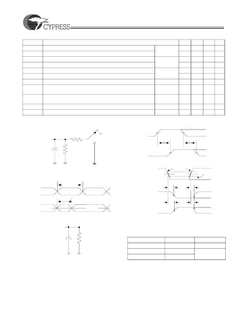
Parameter Measurement Information: V
DD
@ 2.5V
[3,5,6
]
Table 1.
Notes:
3.
4.
C
includes probe and jig capacitance.
Waveform 1 is for an output with internal conditions such that the output is LOW, except when disabled by the output control. Waveform 2 is for an output with
internal conditions such that the output is HIGH except when disabled by the output control.
All input pulses are supplied by generators having the following characteristics: PRR < 10 MHz, Zo = 50
,
t
R
< 2.5 nS, t
F
< 2.5 nS.
Outputs are measured one at a time with one transition per measurement.
t
PLZ
and t
PHZ
are the same as t
DIS
.
t
PZL
and t
PZH
are the same as t
EN
.
t
PLH
and t
PHL
are the same as t
PD
.
5.
6.
7.
8.
9.
AC Switching Characteristics
@ 2.5V V
DD
= 2.5V ± 5%, T
A
=
–
40
°
C to +85
°
C (See
Figure 1
)
Parameter
Description
t
PLH
Propagation Delay
–
Low to High
t
PHL
Propagation Delay
–
High to Low
t
PHZ
Propagation Delay
–
High to High Z
t
PLZ
Propagation Delay
–
Low to High Z
t
R
Output Rise Time
t
F
Output Fall Time
t
SK(0)
Output Skew: Skew between outputs of the same package (in phase) See
Figure 12
t
SK(p)
Pulse Skew: Skew between opposite transitions of the same output
(t
PHL
–
t
PLH
)
t
SK(t)
Package Skew: Skew between outputs of different packages at the
same power supply voltage, temperature and package type.
t
OFF
Delay from OE to Driver Off
t
ON
Delay from OE to Driver on
Min.
1.5
1.5
Typ.
3.8
3.8
5
4
0.4
0.6
Max.
3.5
3.5
Unit
nS
nS
nS
nS
V/nS
V/nS
nS
See
Figure 4
See
Figure 5
See
Figure 4
0.2
See
Figure 11
0.2
nS
See
Figure 13
0.3
nS
5.0
5.0
nS
nS
From Output
Under Test
C
L
= 50 pF
500 ohm
V
SS
Open
2x VDD
500 ohm
Figure 1. Load Circuit
2.5 V
0 V
Input
t
w(20-80)
2.5 V
0 V
1.25 V
1.25 V
Input
t
w(50-50)
1.25 V
Figure 2. Voltage Waveforms
–
Pulse Duration
From Output
Under Test
C
L
= 3 pF
500 ohm
Figure 3. Point-to-Point Load Circuit
Test
t
PLH
/t
PHL
t
PLZ
/t
PZL
t
PHZ
/t
PZH
S1
Open
2
×
V
DD
V
SS
See
Figure 4
See
Figure 5
1.25 V
1.25 V
1.25 V
1.25 V
t
PLH
t
PHL
2.5 V
V
OH
V
OL
0 V
Input
Output
Figure 4. Voltage Waveforms
–
Propagation Delay Times
[9]
Output Control
(low-level enabling)
Waveform 1
S1 at 2 x VDD
2.5 V
Waveform 2
S1 at GND
2.5 V
t
PLZ
t
PHZ
t
PZH
t
PZL
1.25 V
1.25V
0 V
~0 V
V
OL
+ 0.3V
V
OH
- 0.3V
V
OL
V
OH
Z
Z
1.25 V
VOH (min)
VOL
(max)
Figure 5. Voltage Waveforms
–
Enable and Disable Times
[4,7,8]
相关PDF资料 |
PDF描述 |
|---|---|
| CY2CC1810OIT | 1:10 Clock Fanout Buffer with Output Enable |
| CY2CC1810SC | 1:10 Clock Fanout Buffer with Output Enable |
| CY2CC1810SCT | 1:10 Clock Fanout Buffer with Output Enable |
| CY2CC1810SI | 1:10 Clock Fanout Buffer with Output Enable |
| CY2CC1810SIT | 1:10 Clock Fanout Buffer with Output Enable |
相关代理商/技术参数 |
参数描述 |
|---|---|
| CY2CC1810OIT | 制造商:Cypress Semiconductor 功能描述:Clock Fanout Buffer 10-OUT 24-Pin SSOP T/R |
| CY2CC1810OXI | 功能描述:时钟缓冲器 2.5V or 3.3V 200MHz IND RoHS:否 制造商:Texas Instruments 输出端数量:5 最大输入频率:40 MHz 传播延迟(最大值): 电源电压-最大:3.45 V 电源电压-最小:2.375 V 最大功率耗散: 最大工作温度:+ 85 C 最小工作温度:- 40 C 封装 / 箱体:LLP-24 封装:Reel |
| CY2CC1810OXIT | 功能描述:时钟缓冲器 2.5V or 3.3V 200MHz IND RoHS:否 制造商:Texas Instruments 输出端数量:5 最大输入频率:40 MHz 传播延迟(最大值): 电源电压-最大:3.45 V 电源电压-最小:2.375 V 最大功率耗散: 最大工作温度:+ 85 C 最小工作温度:- 40 C 封装 / 箱体:LLP-24 封装:Reel |
| CY2CC1810SC | 制造商:CYPRESS 制造商全称:Cypress Semiconductor 功能描述:1:10 Clock Fanout Buffer with Output Enable |
| CY2CC1810SCT | 制造商:CYPRESS 制造商全称:Cypress Semiconductor 功能描述:1:10 Clock Fanout Buffer with Output Enable |
发布紧急采购,3分钟左右您将得到回复。