- 您现在的位置:买卖IC网 > PDF目录380126 > CY2CC810SC (CYPRESS SEMICONDUCTOR CORP) 1:10 Clock Fanout Buffer PDF资料下载
参数资料
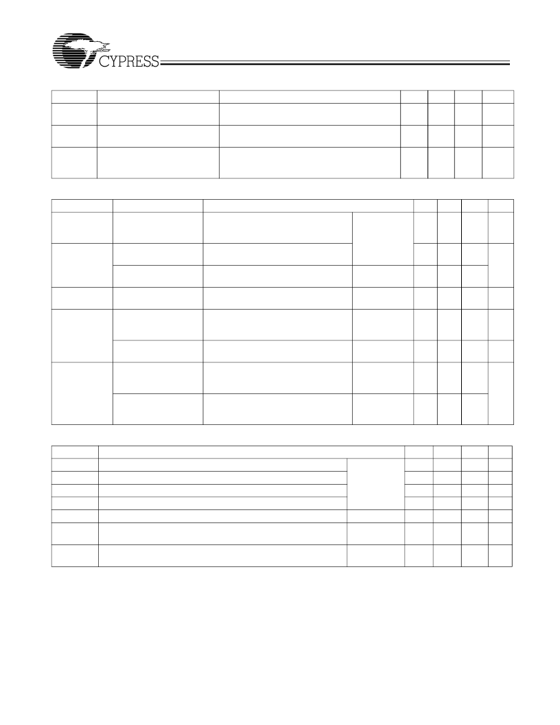
| 型号: | CY2CC810SC |
| 厂商: | CYPRESS SEMICONDUCTOR CORP |
| 元件分类: | 时钟及定时 |
| 英文描述: | 1:10 Clock Fanout Buffer |
| 中文描述: | LOW SKEW CLOCK DRIVER, 10 TRUE OUTPUT(S), 0 INVERTED OUTPUT(S), PDSO20 |
| 封装: | 0.300 INCH, SOIC-20 |
| 文件页数: | 3/7页 |
| 文件大小: | 115K |
| 代理商: | CY2CC810SC |
COMLINK
SERIES
CY2CC810
Document #: 38-07056 Rev. *C
Page 3 of 7
Power Supply Characteristics
(see
Figure 5
)
Parameter
ICC
Description
Test Conditions
Min.
Typ.
Max.
50
Unit
uA
Delta I
CC
Quiescent Power
Supply Current
Dynamic Power Supply Current
(I
DD
@ V
DD
= Max. and V
IN
= V
DD
)
–
(I
DD
@ V
DD
= Max. and V
IN
= V
DD
–
0.6V)
V
DD
= Max.
Input toggling 50% Duty Cycle, Outputs Open
V
DD
= Max.
Input toggling 50% Duty Cycle, Outputs Open
fL = 40 MHZ
I
CCD
0.63
mA/
MHz
mA
I
C
Total Power Supply Current
25
High-frequency Parametrics
Parameter
D
J
Description
Jitter, Deterministic
Test Conditions
Min.
Typ.
Max.
20
Unit
ps
50% duty cycle tW(50
–
50)
The
“
point to point load circuit
”
Output Jitter
–
Input Jitter
50% duty cycle tW(50
–
50)
Standard Load Circuit.
50% duty cycle tW(50
–
50)
The
“
point to point load circuit
”
The
“
point to point load circuit
”
V
IN
= 2.4V/0.0V V
OUT
= 1.7V/0.7V
20% duty cycle tW(20-80)
The
“
point to point load circuit
”
V
IN
= 3.0V/0.0V V
OUT
= 2.3V/0.4V
The
“
point to point load circuit
”
V
IN
= 2.4V/0.0V V
OUT
= 1.7V/0.7V
The
“
point to point load circuit
”
V
IN
= 3.0V/0.0V F = 100 MHz
V
OUT
= 2.0V/0.8V
The
“
point to point load circuit
”
V
IN
= 2.4V/0.0V F = 100 MHz
V
OUT
= 1.7V/0.7V
See
Figure 5
F
max
Maximum frequency
V
DD
= 3.3V
160
MHz
See
Figure 7
650
F
max
2.5V
F
max(20)
Maximum frequency
V
DD
= 2.5 V
Maximum frequency
V
DD
= 3.3 V
See
Figure 7
200
MHz
See
Figure 7
250
MHz
Maximum frequency
V
DD
= 2.5 V
Minimum pulse
V
DD
= 3.3 V
See
Figure 3
200
MHz
t
W
See
Figure 7
1
ns
Minimum pulse
V
DD
= 2.5 V
See
Figure 3
1
AC Switching Characteristics
@ 3.3V V
DD
= 3.3V ±5%, Temperature =
–
40
°
C to +85
°
C
Parameter
t
PLH
Propagation Delay
–
Low to High
t
PHL
Propagation Delay
–
High to Low
t
R
Output Rise Time
t
F
Output Fall Time
t
SK(0)
Output Skew: Skew between outputs of the same package (in phase) See
Figure 10
t
SK(p)
Pulse Skew: Skew between opposite transitions of the same output
(t
PHL
–
t
PLH
).
t
SK(t)
Package Skew: Skew between outputs of different packages at the
same power supply voltage, temperature and package type.
Description
Min.
1.5
1.5
Typ.
2.7
2.7
0.8
0.8
Max.
3.5
3.5
Unit
nS
nS
V/nS
V/nS
nS
nS
See
Figure 4
0.2
0.2
See
Figure 9
See
Figure 11
0.4
nS
相关PDF资料 |
PDF描述 |
|---|---|
| CY2CC810SCT | 1:10 Clock Fanout Buffer |
| CY2CC810SI | 1:10 Clock Fanout Buffer |
| CY2CC810SIT | 1:10 Clock Fanout Buffer |
| CY2CC910OCT | 1:10 Clock Fanout Buffer |
| CY2CC910OIT | 1:10 Clock Fanout Buffer |
相关代理商/技术参数 |
参数描述 |
|---|---|
| CY2CC810SCT | 制造商:CYPRESS 制造商全称:Cypress Semiconductor 功能描述:1:10 Clock Fanout Buffer |
| CY2CC810SI | 制造商:CYPRESS 制造商全称:Cypress Semiconductor 功能描述:1:10 Clock Fanout Buffer |
| CY2CC810SIT | 制造商:CYPRESS 制造商全称:Cypress Semiconductor 功能描述:1:10 Clock Fanout Buffer |
| CY2CC910 | 制造商:CYPRESS 制造商全称:Cypress Semiconductor 功能描述:1:10 Clock Fanout Buffer |
| CY2CC910_05 | 制造商:CYPRESS 制造商全称:Cypress Semiconductor 功能描述:1:10 Clock Fanout Buffer |
发布紧急采购,3分钟左右您将得到回复。