- 您现在的位置:买卖IC网 > PDF目录9599 > CY2SSTV855ZXC (Silicon Laboratories Inc)IC PLL BUF/DRIV I2C 1:5 28TSSOP PDF资料下载
参数资料
| 型号: | CY2SSTV855ZXC |
| 厂商: | Silicon Laboratories Inc |
| 文件页数: | 1/6页 |
| 文件大小: | 0K |
| 描述: | IC PLL BUF/DRIV I2C 1:5 28TSSOP |
| 标准包装: | 50 |
| 系列: | * |
| 类型: | * |
| PLL: | * |
| 主要目的: | * |
| 输入: | * |
| 输出: | * |
| 电路数: | * |
| 比率 - 输入:输出: | * |
| 差分 - 输入:输出: | * |
| 频率 - 最大: | * |
| 电源电压: | * |
| 工作温度: | * |
| 安装类型: | * |
| 封装/外壳: | * |
| 供应商设备封装: | * |
| 包装: | * |
Differential Clock Buffer/Driver
CY2SSTV855
......................... Document #: 38-07459 Rev. *F Page 1 of 6
400 West Cesar Chavez, Austin, TX 78701
1+(512) 416-8500
1+(512) 416-9669
www.silabs.com
Features
Phase-locked loop (PLL) clock distribution for Double
Data Rate Synchronous DRAM applications
1:5 differential outputs
External feedback pins (FBINT, FBINC) are used to
synchronize the outputs to the clock input
SSCG: Spread Aware for electromagnetic
interference (EMI) reduction
28-pin TSSOP package
Conforms to JEDEC DDR specifications
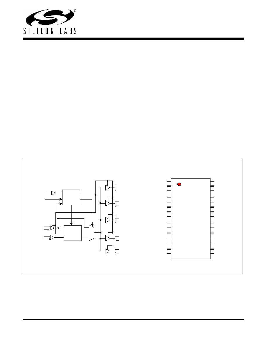
Functional Description
The CY2SSTV855 is a high-performance, very-low-skew,
very-low-jitter zero-delay buffer that distributes a differential
clock input pair (SSTL_2) to four differential (SSTL_2) pairs of
clock outputs and one differential pair of feedback clock
outputs. In support of low power requirements, when
power-down is HIGH, the outputs switch in phase and
frequency with the input clock. When power-down is LOW, all
outputs are disabled to a high-impedance state and the PLL is
shut down.
The device supports a low-frequency power-down mode.
When the input is < 20 MHz, the PLL is disabled and the
outputs are put in the Hi-Z state. When the input frequency is
> 20 MHz, the PLL and outputs are enabled.
When AVDD is tied to ground, the PLL is turned off and
bypassed with the input reference clock gated to the outputs.
The Cypress CY2SSTV855 is Spread Aware and supports
tracking of Spread Spectrum clock inputs to reduce EMI
Block Diagram
Pin Configuration
28-pin TSSOP
1
2
3
4
5
6
7
8
9
10
11
12
13
14
28
27
26
25
24
23
22
21
20
19
18
17
16
15
GND
YT3
VDDQ
FBOUTT
YT2
YC2
GND
VDDQ
FBOUTC
YC3
VDDQ
PWRDWN
FBINT
FBINC
GND
YT0
VDDQ
AGND
YT1
YC1
GND
VDDQ
AVDD
YC0
VDDQ
GND
CLKINT
CLKINC
CY2S
STV855
FBOUTT
FBOUTC
YT0
YC0
YC3
YT3
PLL
PWRDWN
YC2
YT2
YT1
YC1
Powerdown
and test
logic
AVDD
CLKINT
CLKINC
FBINT
FBINC
相关PDF资料 |
PDF描述 |
|---|---|
| ICL3245EIA | IC 3DRVR/5RCVR RS232 3V 28-SSOP |
| VE-223-MX-F2 | CONVERTER MOD DC/DC 24V 75W |
| VE-BWN-MW-F4 | CONVERTER MOD DC/DC 18.5V 100W |
| VE-22M-MY-S | CONVERTER MOD DC/DC 10V 50W |
| VE-22L-MY-S | CONVERTER MOD DC/DC 28V 50W |
相关代理商/技术参数 |
参数描述 |
|---|---|
| CY2SSTV855ZXCT | 功能描述:时钟缓冲器 2.5V 170MHz 1:5 Differential DDR PLL RoHS:否 制造商:Texas Instruments 输出端数量:5 最大输入频率:40 MHz 传播延迟(最大值): 电源电压-最大:3.45 V 电源电压-最小:2.375 V 最大功率耗散: 最大工作温度:+ 85 C 最小工作温度:- 40 C 封装 / 箱体:LLP-24 封装:Reel |
| CY2SSTV855ZXI | 功能描述:时钟缓冲器 DDR1 Clock PLL RoHS:否 制造商:Texas Instruments 输出端数量:5 最大输入频率:40 MHz 传播延迟(最大值): 电源电压-最大:3.45 V 电源电压-最小:2.375 V 最大功率耗散: 最大工作温度:+ 85 C 最小工作温度:- 40 C 封装 / 箱体:LLP-24 封装:Reel |
| CY2SSTV855ZXIT | 功能描述:时钟缓冲器 DDR1 Clock PLL RoHS:否 制造商:Texas Instruments 输出端数量:5 最大输入频率:40 MHz 传播延迟(最大值): 电源电压-最大:3.45 V 电源电压-最小:2.375 V 最大功率耗散: 最大工作温度:+ 85 C 最小工作温度:- 40 C 封装 / 箱体:LLP-24 封装:Reel |
| CY2SSTV857 | 制造商:CYPRESS 制造商全称:Cypress Semiconductor 功能描述:Differential Clock Buffer/Driver DDR333/PC2700-Compliant |
| CY2SSTV857-27 | 制造商:未知厂家 制造商全称:未知厂家 功能描述:Clocks and Buffers |
发布紧急采购,3分钟左右您将得到回复。