- 您现在的位置:买卖IC网 > PDF目录380142 > CY39050V208-83NI (Cypress Semiconductor Corp.) CPLDs at FPGA Densities PDF资料下载
参数资料
| 型号: | CY39050V208-83NI |
| 厂商: | Cypress Semiconductor Corp. |
| 英文描述: | CPLDs at FPGA Densities |
| 中文描述: | CPLD器件在FPGA的密度 |
| 文件页数: | 12/86页 |
| 文件大小: | 1235K |
| 代理商: | CY39050V208-83NI |
第1页第2页第3页第4页第5页第6页第7页第8页第9页第10页第11页当前第12页第13页第14页第15页第16页第17页第18页第19页第20页第21页第22页第23页第24页第25页第26页第27页第28页第29页第30页第31页第32页第33页第34页第35页第36页第37页第38页第39页第40页第41页第42页第43页第44页第45页第46页第47页第48页第49页第50页第51页第52页第53页第54页第55页第56页第57页第58页第59页第60页第61页第62页第63页第64页第65页第66页第67页第68页第69页第70页第71页第72页第73页第74页第75页第76页第77页第78页第79页第80页第81页第82页第83页第84页第85页第86页
Delta39K ISR
CPLD Family
Document #: 38-03039 Rev. *H
Page 12 of 86
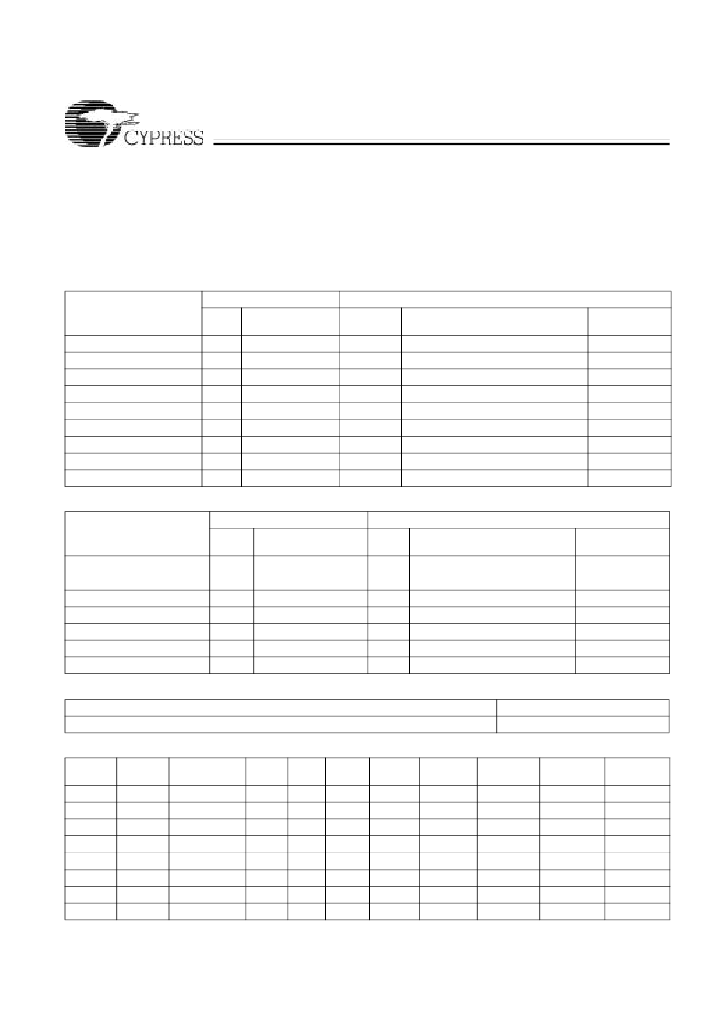
Table 6
describes the valid phase shift options that can be
used with or without an external feedback.
Table 7
is an example of the effect of all the available divide
and phase shift options on a VCO output of 250 MHz. It also
shows the effect of division on the duty cycle of the resultant
clock. Note that the duty cycle is 50-50 when a VCO output is
divided by an even number. Also note that the phase shift
applies to the VCO output and not to the divided output.
For more details on the architecture and operation of this PLL
please refer to the application note entitled
“Delta39K PLL and
Clock Tree”.
Table 4. Valid PLL Multiply and Divide Options—without External Feedback
Input Frequency
(GCLK[0])
f
PLLI
(MHz)
DC–12.5
100–133
50–133
33.3–88.7
25–66
20–53.2
16.6–44.3
12.5–33
12.5–16.625
Valid Multiply Options
VCO Output
Frequency (MHz)
N/A
1
100–133
2
100–266
3
100–266
4
100–266
5
100–266
6
100–266
8
100–266
16
200–266
Valid Divide Options
Output Frequency (INTCLK[3:0])
f
PLLO
(MHz)
DC–12.5
6.25–133
6.25–266
6.25–266
6.25–266
6.25–266
6.25–266
6.25–266
6.25–266
Value
Value
N/A
1–6, 8, 16
1–6, 8, 16
1–6, 8, 16
1–6, 8, 16
1–6, 8, 16
1–6, 8, 16
1–6, 8, 16
1–6, 8, 16
Off-chip Clock
Frequency
DC–6.25
3.125–66
3.125–133
3.1–266
3.125–133
3.1–133
3.1–133
3.125–133
3.125–133
N/A
Table 5. Valid PLL Multiply and Divide Options—With External Feedback
Input (GCLK) Frequency
f
PLLI
(MHz)
50–133
25–66.5
16.67–44.33
12.5–33.25
12.5–26.6
12.5–22.17
12.5–16.63
Valid Multiply Options
VCO Output
Frequency (MHz)
1
100–266
1
100–266
1
100–266
1
100–266
1
125–266
1
150–266
1
200–266
Valid Divide Options
Output (INTCLK) Frequency
f
PLLO
(MHz)
100–266
50–133
33.33–88.66
25–66.5
25–53.2
25–44.34
25–33.25
Value
Value
1
2
3
4
5
6
8
Off-chip Clock
Frequency
50–133
25–66.5
16.67–44.33
12.5–33.25
12.5–26.6
12.5–22.17
12.5–16.63
Table 6. Recommended PLL Phase Shift Options
Without External Feedback
With External Feedback
0°,45°, 90°, 135°, 180°, 225°, 270°, 315°
0°
Table 7. Timing of Clock Phases for all Divide Options for a V
CO
Output Frequency of 250 MHz
Divide
Factor
(ns)
Duty Cycle%
(ns)
(ns)
1
4
40–60
0
0.5
2
8
50
0
0.5
3
12
33–67
0
0.5
4
16
50
0
0.5
5
20
40–60
0
0.5
6
24
50
0
0.5
8
32
50
0
0.5
16
64
50
0
0.5
Period
0°
45°
90°
(ns)
1.0
1.0
1.0
1.0
1.0
1.0
1.0
1.0
135°
(ns)
1.5
1.5
1.5
1.5
1.5
1.5
1.5
1.5
180°
(ns)
2.0
2.0
2.0
2.0
2.0
2.0
2.0
2.0
225°
(ns)
2.5
2.5
2.5
2.5
2.5
2.5
2.5
2.5
270°
(ns)
3.0
3.0
3.0
3.0
3.0
3.0
3.0
3.0
315°
(ns)
3.5
3.5
3.5
3.5
3.5
3.5
3.5
3.5
相关PDF资料 |
PDF描述 |
|---|---|
| CY39030Z256-125MGC | CPLDs at FPGA Densities |
| CY39030Z256-125MGI | CPLDs at FPGA Densities |
| CY39030Z256-125NC | CPLDs at FPGA Densities |
| CY39030Z256-125NI | CPLDs at FPGA Densities |
| CY39030Z256-125NTC | CPLDs at FPGA Densities |
相关代理商/技术参数 |
参数描述 |
|---|---|
| CY39050V208-83NTXC | 功能描述:IC CPLD 50K GATE 208BQFP RoHS:是 类别:集成电路 (IC) >> 嵌入式 - CPLD(复杂可编程逻辑器件) 系列:Delta 39K™ ISR™ 标准包装:24 系列:CoolRunner II 可编程类型:系统内可编程 最大延迟时间 tpd(1):7.1ns 电压电源 - 内部:1.7 V ~ 1.9 V 逻辑元件/逻辑块数目:24 宏单元数:384 门数:9000 输入/输出数:173 工作温度:0°C ~ 70°C 安装类型:表面贴装 封装/外壳:208-BFQFP 供应商设备封装:208-PQFP(28x28) 包装:托盘 |
| CY39050V208-83NTXI | 功能描述:IC CPLD 50K GATE 208BQFP RoHS:是 类别:集成电路 (IC) >> 嵌入式 - CPLD(复杂可编程逻辑器件) 系列:Delta 39K™ ISR™ 标准包装:24 系列:CoolRunner II 可编程类型:系统内可编程 最大延迟时间 tpd(1):7.1ns 电压电源 - 内部:1.7 V ~ 1.9 V 逻辑元件/逻辑块数目:24 宏单元数:384 门数:9000 输入/输出数:173 工作温度:0°C ~ 70°C 安装类型:表面贴装 封装/外壳:208-BFQFP 供应商设备封装:208-PQFP(28x28) 包装:托盘 |
| CY39050V484-125BBC | 制造商:CYPRESS 制造商全称:Cypress Semiconductor 功能描述:CPLDs at FPGA Densities |
| CY39050V484-125BBI | 制造商:CYPRESS 制造商全称:Cypress Semiconductor 功能描述:CPLDs at FPGA Densities |
| CY39050Z208-125BBC | 制造商:CYPRESS 制造商全称:Cypress Semiconductor 功能描述:CPLDs at FPGA Densities |
发布紧急采购,3分钟左右您将得到回复。