- 您现在的位置:买卖IC网 > PDF目录380137 > CY39050Z484-83MGI (Cypress Semiconductor Corp.) CPLDs at FPGA Densities PDF资料下载
参数资料
| 型号: | CY39050Z484-83MGI |
| 厂商: | Cypress Semiconductor Corp. |
| 英文描述: | CPLDs at FPGA Densities |
| 中文描述: | CPLD器件在FPGA的密度 |
| 文件页数: | 4/86页 |
| 文件大小: | 1235K |
| 代理商: | CY39050Z484-83MGI |
第1页第2页第3页当前第4页第5页第6页第7页第8页第9页第10页第11页第12页第13页第14页第15页第16页第17页第18页第19页第20页第21页第22页第23页第24页第25页第26页第27页第28页第29页第30页第31页第32页第33页第34页第35页第36页第37页第38页第39页第40页第41页第42页第43页第44页第45页第46页第47页第48页第49页第50页第51页第52页第53页第54页第55页第56页第57页第58页第59页第60页第61页第62页第63页第64页第65页第66页第67页第68页第69页第70页第71页第72页第73页第74页第75页第76页第77页第78页第79页第80页第81页第82页第83页第84页第85页第86页
Delta39K ISR
CPLD Family
Document #: 38-03039 Rev. *H
Page 4 of 86
figure the devices without having design changes cause
pinout or timing changes in most cases. The Cypress ISR
function is implemented through a JTAG-compliant serial
interface. Data is shifted in and out through the TDI and TDO
pins respectively. Superior routability, simple timing, and the
ISR allows users to change existing logic designs while simul-
taneously fixing pinout assignments and maintaining system
performance.
The entire family features JTAG for ISR and boundary scan,
and is compatible with the PCI Local Bus specification,
meeting the electrical and timing requirements. The Delta39K
family also features user programmable bus-hold and slew
rate control capabilities on each I/O pin.
AnyVolt Interface
All Delta39KV devices feature an on-chip regulator, which
accepts 3.3V or 2.5V on the V
CC
supply pins and steps it down
to 1.8V internally, the voltage level at which the core operates.
With Delta39K’s AnyVolt technology, the I/O pins can be
connected to either 1.8V, 2.5V, or 3.3V. All Delta39K devices
are 3.3V-tolerant regardless of V
CCIO
or V
CC
settings.
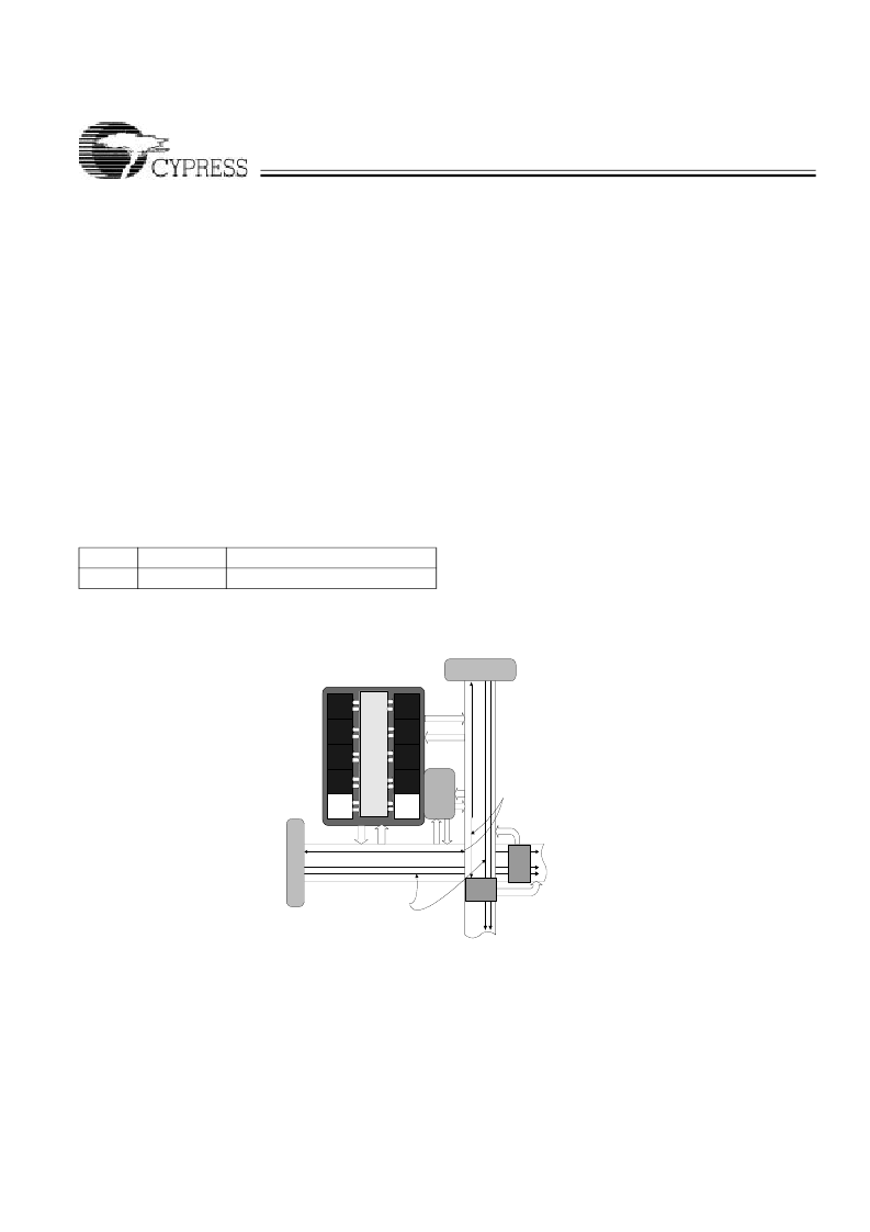
Global Routing Description
The routing architecture of the Delta39K is made up of
horizontal and vertical (H and V) routing channels. These
routing channels allow signals from each of the Delta39K
architectural components to communicate with one another. In
addition to the horizontal and vertical routing channels that
interconnect the I/O banks, channel memory blocks, and logic
block clusters, each LBC contains a Programmable Inter-
connect Matrix
(PIM), which is used to route signals
among the logic blocks and the cluster memory blocks.
Figure 2
is a block diagram of the routing channels that
interface within the Delta39K architecture. The LBC is exactly
the same for every member of the Delta39K CPLD family.
Logic Block Cluster (LBC)
The Delta39K architecture consists of several logic block
clusters, each of which have eight Logic Blocks (LB) and two
cluster memory blocks connected via a Programmable Inter-
connect Matrix (PIM) as shown in
Figure 3
. Each cluster
memory block consists of 8-Kbit single-port RAM, which is
configurable as synchronous or asynchronous. The cluster
memory blocks can be cascaded with other cluster memory
blocks within the same LBC as well as other LBCs to
implement larger memory functions. If a cluster memory block
is not specifically utilized by the designer, Cypress’s
Warp
software can automatically use it to implement large blocks of
logic.
All LBCs interface with each other via horizontal and vertical
routing channels.
Note:
5.
For HSTL only.
Table 1.
Device
39KV
V
CC
V
CCIO
3.3V or 2.5V
3.3V or 2.5V or 1.8V or 1.5V
[5]
LB
Cluster
PIM
Cluster
Memory
Block
LB
LB
LB
LB
Cluster
Memory
Block
LB
LB
LB
Channel
Memory
Block
I/O Block
I
Channel memory
outputs drive
dedicated tracks in the
horizontal and vertical
routing channels
H-to-V
PIM
V-to-H
PIM
Pin inputs from the I/O cells
drive dedicated tracks in the
horizontal and vertical routing
channels
72
72
64
64
Figure 2. Delta39K Routing Interface
相关PDF资料 |
PDF描述 |
|---|---|
| CY39050Z484-83NC | CPLDs at FPGA Densities |
| CY39050Z484-83NI | CPLDs at FPGA Densities |
| CY39050Z484-83NTC | CPLDs at FPGA Densities |
| CY39050Z484-83NTI | CPLDs at FPGA Densities |
| CY39050Z676-125MBC | CPLDs at FPGA Densities |
相关代理商/技术参数 |
参数描述 |
|---|---|
| CY39050Z676-125BBC | 制造商:CYPRESS 制造商全称:Cypress Semiconductor 功能描述:CPLDs at FPGA Densities |
| CY39050Z676-125BBI | 制造商:CYPRESS 制造商全称:Cypress Semiconductor 功能描述:CPLDs at FPGA Densities |
| CY39050Z676-125BGC | 制造商:CYPRESS 制造商全称:Cypress Semiconductor 功能描述:CPLDs at FPGA Densities |
| CY39050Z676-125BGI | 制造商:CYPRESS 制造商全称:Cypress Semiconductor 功能描述:CPLDs at FPGA Densities |
| CY39100V208-125BBC | 制造商:CYPRESS 制造商全称:Cypress Semiconductor 功能描述:CPLDs at FPGA Densities |
发布紧急采购,3分钟左右您将得到回复。