- 您现在的位置:买卖IC网 > PDF目录380136 > CY39100V388-125BBC (Cypress Semiconductor Corp.) CPLDs at FPGA Densities PDF资料下载
参数资料
| 型号: | CY39100V388-125BBC |
| 厂商: | Cypress Semiconductor Corp. |
| 英文描述: | CPLDs at FPGA Densities |
| 中文描述: | CPLD器件在FPGA的密度 |
| 文件页数: | 14/86页 |
| 文件大小: | 1235K |
| 代理商: | CY39100V388-125BBC |
第1页第2页第3页第4页第5页第6页第7页第8页第9页第10页第11页第12页第13页当前第14页第15页第16页第17页第18页第19页第20页第21页第22页第23页第24页第25页第26页第27页第28页第29页第30页第31页第32页第33页第34页第35页第36页第37页第38页第39页第40页第41页第42页第43页第44页第45页第46页第47页第48页第49页第50页第51页第52页第53页第54页第55页第56页第57页第58页第59页第60页第61页第62页第63页第64页第65页第66页第67页第68页第69页第70页第71页第72页第73页第74页第75页第76页第77页第78页第79页第80页第81页第82页第83页第84页第85页第86页
Delta39K ISR
CPLD Family
Document #: 38-03039 Rev. *H
Page 14 of 86
IEEE 1149.1-compliant JTAG Operation
The Delta39K family has an IEEE 1149.1 JTAG interface for
both Boundary Scan and ISR operations.
Four dedicated pins are reserved on each device for use by
the Test Access Port (TAP).
Boundary Scan
The Delta39K family supports Bypass, Sample/Preload,
Extest, Intest, Idcode and Usercode boundary scan instruc-
tions. The JTAG interface is shown in
Figure 11
.
In-System Reprogramming (ISR)
In-System Reprogramming is the combination of the capability
to program or reprogram a device on-board, and the ability to
support design changes without changing the system timing
or device pinout. This combination means design changes
during debug or field upgrades do not cause board respins.
The Delta39K family implements ISR by providing a JTAG
compliant interface for on-board programming, robust routing
resources for pinout flexibility, and a simple timing model for
consistent system performance.
Configuration
Each device of the Delta39K family is available in a volatile and
a Self-Boot package. Cypress’s CPLD boot EEPROM is used
to store configuration data for the volatile solution and an
embedded on-chip FLASH memory device is used for the Self-
Boot solution.
For volatile Delta39K packages, programming is defined as
the loading of a user’s design into the external CPLD boot
EEPROM. For Self-Boot Delta39K packages, programming is
defined as the loading of a user’s design into the on-chip
FLASH internal to the Delta39K package. Configuration is
defined as the loading of a user’s design into the Delta39K die.
Channel
RAM
4
GCLK[3:0]
LB 0
PIM
RAM
LB 5
LB 4
RAM
LB 6
LB 7
LB 2
LB 3
Cluster
LB 1
Channel
RAM
4
LB 0
PIM
RAM
LB 5
LB 4
RAM
LB 6
LB 7
LB 2
LB 3
LB 1
Channel
RAM
4
LB 0
PIM
RAM
LB 5
LB 4
RAM
LB 6
LB 7
LB 2
LB 3
LB 1
Channel
RAM
4
LB 0
PIM
8 Kb
LB 5
LB 4
8 Kb
LB 6
LB 7
LB 2
LB 3
LB 1
Channel
RAM
4
GCLK[3:0]
LB 0
PIM
RAM
LB 5
LB 4
RAM
LB 6
LB 7
LB 2
LB 3
LB 1
4
LB 0
PIM
LB 5
LB 4
RAM
LB 6
LB 7
LB 2
LB 3
RAM
LB 1
4
LB 0
PIM
RAM
LB 5
LB 4
RAM
LB 6
LB 7
LB 2
LB 3
LB 1
Channel
RAM
4
LB 0
PIM
RAM
LB 5
LB 4
Cluster
RAM
LB 6
LB 7
LB 2
LB 3
LB 1
Channel
RAM
4
GCLK[3:0]
LB 0
PIM
RAM
LB 5
LB 4
RAM
LB 6
LB 7
LB 2
LB 3
LB 1
Channel
RAM
4
LB 0
PIM
RAM
LB 5
LB 4
RAM
LB 6
LB 7
LB 2
LB 3
LB 1
Channel
RAM
4
LB 0
PIM
RAM
LB 5
LB 4
RAM
LB 6
LB 7
LB 2
LB 3
LB 1
Channel
RAM
4
LB 0
PIM
RAM
LB 5
LB 4
RAM
LB 6
LB 7
LB 2
LB 3
LB 1
Channel
RAM
Channel
RAM
t
MCS
t
PD
t
SCS
t
MCCO
t
SCS2
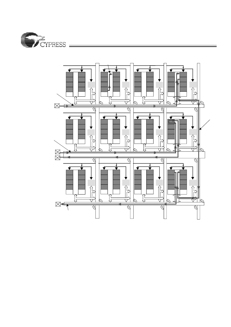
Figure 10. Timing Model for 39K100 Device
相关PDF资料 |
PDF描述 |
|---|---|
| CY39100V388-125BBI | CPLDs at FPGA Densities |
| CY39100V388-125BGC | CPLDs at FPGA Densities |
| CY39100V388-125BGI | CPLDs at FPGA Densities |
| CY39100V388-125MBC | CPLDs at FPGA Densities |
| CY39100V388-125MBI | CPLDs at FPGA Densities |
相关代理商/技术参数 |
参数描述 |
|---|---|
| CY39100V388-125MGC | 制造商:CYPRESS 制造商全称:Cypress Semiconductor 功能描述:CPLDs at FPGA Densities |
| CY39100V388-181MBC | 制造商:CYPRESS 制造商全称:Cypress Semiconductor 功能描述:CPLDs at FPGA Densities |
| CY39100V388-181MGC | 制造商:CYPRESS 制造商全称:Cypress Semiconductor 功能描述:CPLDs at FPGA Densities |
| CY39100V388-181NC | 制造商:CYPRESS 制造商全称:Cypress Semiconductor 功能描述:CPLDs at FPGA Densities |
| CY39100V388-233MGC | 制造商:CYPRESS 制造商全称:Cypress Semiconductor 功能描述:CPLDs at FPGA Densities |
发布紧急采购,3分钟左右您将得到回复。