- 您现在的位置:买卖IC网 > PDF目录380137 > CY39200V388-200BBI (Cypress Semiconductor Corp.) CPLDs at FPGA Densities PDF资料下载
参数资料
| 型号: | CY39200V388-200BBI |
| 厂商: | Cypress Semiconductor Corp. |
| 英文描述: | CPLDs at FPGA Densities |
| 中文描述: | CPLD器件在FPGA的密度 |
| 文件页数: | 17/86页 |
| 文件大小: | 1235K |
| 代理商: | CY39200V388-200BBI |
第1页第2页第3页第4页第5页第6页第7页第8页第9页第10页第11页第12页第13页第14页第15页第16页当前第17页第18页第19页第20页第21页第22页第23页第24页第25页第26页第27页第28页第29页第30页第31页第32页第33页第34页第35页第36页第37页第38页第39页第40页第41页第42页第43页第44页第45页第46页第47页第48页第49页第50页第51页第52页第53页第54页第55页第56页第57页第58页第59页第60页第61页第62页第63页第64页第65页第66页第67页第68页第69页第70页第71页第72页第73页第74页第75页第76页第77页第78页第79页第80页第81页第82页第83页第84页第85页第86页
Delta39K ISR
CPLD Family
Document #: 38-03039 Rev. *H
Page 17 of 86
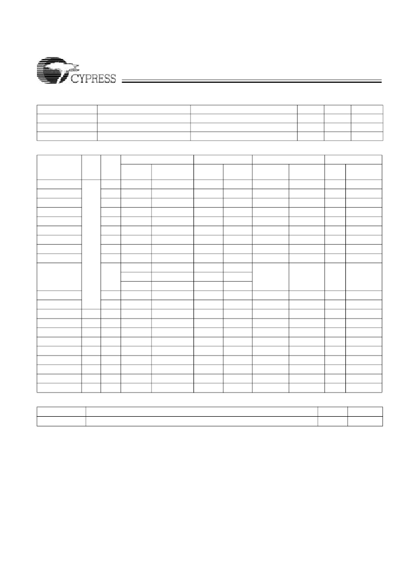
Capacitance
Power-up Sequence Requirements
Upon power-up, all the outputs remain three-stated until all
the V
pins
have powered-up to the nominal voltage and
the part has completed configuration.
The part will not start configuration until V
CC
, V
CCIO
,
V
CCJTAG
, V
CCCNFG
, V
CCPLL
and V
CCPRG
have reached
nominal voltage.
V
CC
pins can be powered up in any order. This includes
V
CC
, V
CCIO
, V
CCJTAG
, V
CCCNFG
, V
CCPLL
and V
CCPRG
.
All V
s on a bank should be tied to the same potential
and powered up together.
All V
s (even the unused banks) need to be powered up
to at least 1.5V before configuration has completed.
Maximum ramp time for all V
CC
s should be 0V to nominal
voltage in 100 ms.
Notes:
9.
PCI spec (rev 2.2) requires the IDSEL pin to have capacitance less than or equal to 8 pF. Delta39K Pin Tables starting from page 45, identify all the I/O pins in
a given package, which can be used as IDSEL in a PCI design. All other I/O pins meet the PCI requirement of capacitance less than or equal to 10 pf.
10. The number of I/Os which can be used in each I/O bank depends on the type of I/O standards and the number of V
CCIO
and GND pins being used. Please refer
to the application note titled
“Delta39K and Quantum38K I/O Standards and Configurations”
for details.
The source current limit per I/O bank per Vccio pin is 165 mA.
The sink current limit per I/O bank per GND pin is 230 mA.
11.
See “Power-up Sequence Requirements” below for V
CCIO
requirement.
12. 25W resistor terminated to termination voltage of 1.5V.
Parameter
Description
Test Conditions
Min.
Max.
10
12
8
Unit
pF
pF
pF
C
I/O
C
CLK
C
PCI
Input/Output Capacitance
Clock Signal Capacitance
PCI-compliant
[9]
Capacitance
V
in
= V
CCIO
@ f = 1 MHz 25°C
V
in
= V
CCIO
@ f = 1 MHz 25°C
V
in
= V
CCIO
@ f = 1 MHz 25°C
5
DC Characteristics (I/O)
[10]
I/O Standards
LVTTL –2 mA
LVTTL –4 mA
LVTTL –6 mA
LVTTL –8 mA
LVTTL –12 mA
LVTTL –16 mA
LVTTL –24 mA
LVCMOS
LVCMOS3
V
(V)
N/A
V
(V)
3.3
3.3
3.3
3.3
3.3
3.3
3.3
3.3
3.0
2.5
V
OH
(V)
V
OL
(V)
V
IH
(V)
V
IL
(V)
@ I
OH
=
–2 mA
–4 mA
–6 mA
–8 mA
–12 mA
–16 mA
–24 mA
–0.1 mA
–0.1 mA
–0.1 mA
–1.0 mA
–2.0 mA
–2 mA
–0.5 mA
V
OH
(min.)
2.4
2.4
2.4
2.4
2.4
2.4
2.4
V
CCIO
– 0.2V
V
CCIO
– 0.2V
2.1
2.0
1.7
V
CCIO
– 0.45V
0.9V
CCIO
@ I
OL
=
2 mA
4 mA
6 mA
8 mA
12 mA
16 mA
24 mA
0.1 mA
0.1 mA
0.1 mA
1.0 mA
2.0 mA
2.0 mA
1.5 mA
36 mA
[12]
8 mA
16 mA
7.6 mA
V
(max.)
0.4
0.4
0.4
0.4
0.4
0.4
0.4
0.2
0.2
0.2
0.4
0.7
0.45
0.1V
CCIO
0.6
0.7
0.5
0.54
0.35
0.4
0.4
0.4
0.4
Min.
2.0V
2.0V
2.0V
2.0V
2.0V
2.0V
2.0V
2.0V
2.0V
1.7V
Max.
Min.
Max.
0.8V
0.8V
0.8V
0.8V
0.8V
0.8V
0.8V
0.8V
0.8V
0.7V
V
CCIO
+ 0.3 –0.3V
V
CCIO
+ 0.3 –0.3V
V
CCIO
+ 0.3 –0.3V
V
CCIO
+ 0.3 –0.3V
V
CCIO
+ 0.3 –0.3V
V
CCIO
+ 0.3 –0.3V
V
CCIO
+ 0.3 –0.3V
V
CCIO
+ 0.3 –0.3V
V
CCIO
+ 0.3 –0.3V
V
CCIO
+ 0.3 –0.3V
LVCMOS2
LVCMOS18
3.3V PCI
GTL+
SSTL3 I
SSTL3 II
SSTL2 I
SSTL2 II
HSTL I
HSTL II
HSTL III
HSTL IV
1.8
3.3
[11]
0.65V
CCIO
0.5V
CCIO
V
REF
+ 0.2
V
REF
+ 0.2
V
REF
+ 0.2
V
REF
+ 0.18 V
CCIO
+ 0.3 –0.3V V
REF
– 0.18
V
REF
+ 0.18 V
CCIO
+ 0.3 –0.3V V
REF
– 0.18
V
REF
+ 0.1
V
CCIO
+ 0.3 –0.3V
V
REF
+ 0.1
V
CCIO
+ 0.3 –0.3V
V
REF
+ 0.1
V
CCIO
+ 0.3 –0.3V
V
REF
+ 0.1
V
CCIO
+ 0.3 –0.3V
V
CCIO
+ 0.3 –0.3V
V
CCIO
+ 0.5 –0.5V
0.35V
CCIO
0.3V
CCIO
V
REF
– 0.2
V
REF
– 0.2
V
REF
– 0.2
1.0
1.5
1.5
1.25
1.25
0.75
0.75
0.9
0.9
3.3
3.3
2.5
2.5
1.5
1.5
1.5
1.5
–8 mA
–16 mA
–7.6 mA V
CCIO
– 0.62V
–15.2 mA V
CCIO
– 0.43V 15.2 mA
–8 mA
V
CCIO
– 0.4V
–16 mA
V
CCIO
– 0.4V
–8 mA
V
CCIO
– 0.4V
–8 mA
V
CCIO
– 0.4V
V
CCIO
– 1.1V
V
CCIO
– 0.9V
V
CCIO
+ 0.3 –0.3V
V
CCIO
+ 0.3 –0.3V
8 mA
16 mA
24 mA
48 mA
V
REF
– 0.1
V
REF
– 0.1
V
REF
– 0.1
V
REF
– 0.1
Configuration Parameters
Parameter
t
RECONFIG
Description
Min.
200
Unit
ns
Reconfig
pin LOW time before it goes HIGH
相关PDF资料 |
PDF描述 |
|---|---|
| CY39200V388-200BGC | CPLDs at FPGA Densities |
| CY39200V388-200BGI | CPLDs at FPGA Densities |
| CY39200V388-200MBC | CPLDs at FPGA Densities |
| CY39200V388-200MBI | CPLDs at FPGA Densities |
| CY39200V388-200MGC | CPLDs at FPGA Densities |
相关代理商/技术参数 |
参数描述 |
|---|---|
| CY39200V388-233MGC | 制造商:CYPRESS 制造商全称:Cypress Semiconductor 功能描述:CPLDs at FPGA Densities |
| CY39200V388-233MGI | 制造商:CYPRESS 制造商全称:Cypress Semiconductor 功能描述:CPLDs at FPGA Densities |
| CY39200V388-233NTC | 制造商:CYPRESS 制造商全称:Cypress Semiconductor 功能描述:CPLDs at FPGA Densities |
| CY39200V388-83MGC | 制造商:Cypress Semiconductor 功能描述: |
| CY39200V484-125BBC | 制造商:CYPRESS 制造商全称:Cypress Semiconductor 功能描述:CPLDs at FPGA Densities |
发布紧急采购,3分钟左右您将得到回复。