- 您现在的位置:买卖IC网 > PDF目录380137 > CY39200V388-200BGC (Cypress Semiconductor Corp.) CPLDs at FPGA Densities PDF资料下载
参数资料
| 型号: | CY39200V388-200BGC |
| 厂商: | Cypress Semiconductor Corp. |
| 英文描述: | CPLDs at FPGA Densities |
| 中文描述: | CPLD器件在FPGA的密度 |
| 文件页数: | 11/86页 |
| 文件大小: | 1235K |
| 代理商: | CY39200V388-200BGC |
第1页第2页第3页第4页第5页第6页第7页第8页第9页第10页当前第11页第12页第13页第14页第15页第16页第17页第18页第19页第20页第21页第22页第23页第24页第25页第26页第27页第28页第29页第30页第31页第32页第33页第34页第35页第36页第37页第38页第39页第40页第41页第42页第43页第44页第45页第46页第47页第48页第49页第50页第51页第52页第53页第54页第55页第56页第57页第58页第59页第60页第61页第62页第63页第64页第65页第66页第67页第68页第69页第70页第71页第72页第73页第74页第75页第76页第77页第78页第79页第80页第81页第82页第83页第84页第85页第86页
Delta39K ISR
CPLD Family
Document #: 38-03039 Rev. *H
Page 11 of 86
Programmable Bus Hold
On each I/O pin, user-programmable-bus-hold is included.
Bus-hold, which is an improved version of the popular internal
pull-up resistor, is a weak latch connected to the pin that does
not degrade the device’s performance. As a latch, bus-hold
maintains the last state of a pin when the pin is placed in a
high-impedance state, thus reducing system noise in bus-
interface applications. Bus-hold additionally allows unused
device pins to remain unconnected on the board, which is
particularly useful during prototyping as designers can route
new signals to the device without cutting trace connections to
V
CC
or GND. For more information, see the application note
titled
“Understanding Bus-Hold–A Feature of Cypress
CPLDs.”
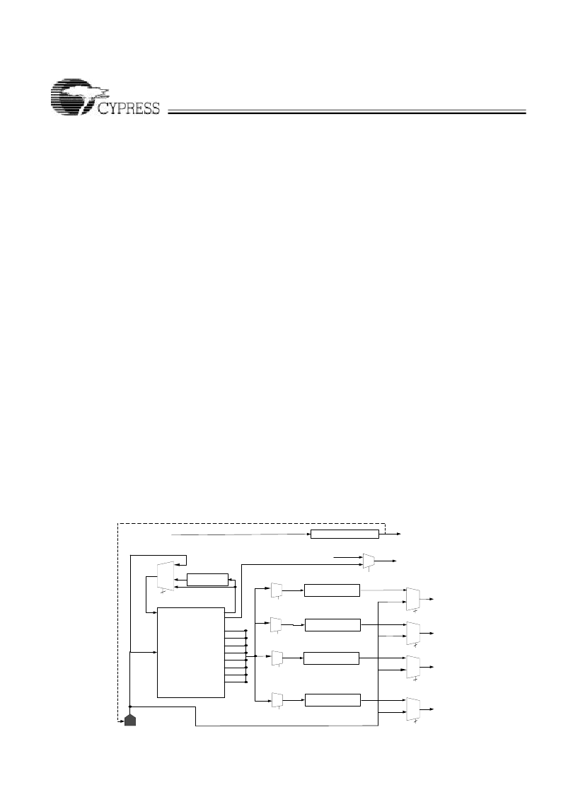
Clocks
Delta39K has four dedicated clock input pins (GCLK[3:0]) to
accept system clocks. One of these clocks (GCLK[0]) may be
selected to drive an on-chip phase-locked loop (PLL) for
frequency modulation (see
Figure 9
for details).
The global clock tree for a Delta39K device can be driven by
a combination of the dedicated clock pins and/or the PLL-
derived clocks. The global clock tree consists of four global
clocks that go to every macrocell, memory block, and I/O cell.
Clock Tree Distribution
The global clock tree performs two primary functions. First, the
clock tree generates the four global clocks by multiplexing four
dedicated clocks from the package pins and four PLL driven
clocks. Second, the clock tree distributes the four global clocks
to every cluster, channel memory, and I/O block on the die.
The global clock tree is designed such that the clock skew is
minimized while maintaining an acceptable clock delay.
Spread Aware PLL
Each device in the Delta39K family features an on-chip PLL
designed using Spread Aware technology for low EMI applica-
tions. In general, PLLs are used to implement time-division-
multiplex circuits to achieve higher performance with fewer
device resources.
For example, a system that operates on a 32-bit data path that
runs at 40 MHz can be implemented with 16-bit circuitry that
runs internally at 80 MHz. PLLs can also be used to take
advantage of the positioning of the internally generated clock
edges to shift performance towards improved setup, hold or
clock-to-out times.
There are several frequency multiply (X1, X2, X3, X4, X5, X6,
X8, X16) and divide (/1, /2, /3, /4, /5, /6, /8, /16) options
available to create a wide range of clock frequencies from a
single clock input (GCLK[0]). For increased flexibility, there are
seven phase shifting options which allow clock skew/deskew
by 45°, 90°, 135°, 180°, 225°, 270°, or 315°.
The Spread Aware feature refers to the ability of the PLL to
track a spread-spectrum input clock such that its spread is
seen on the output clock with the PLL staying locked. The total
amount of spread on the input clock should be limited to 0.6%
of the fundamental frequency. Spread Aware feature is
supported only with X1, X2, and X4 multiply options.
The Voltage Controlled Oscillator (VCO), the core of the
Delta39K PLL is designed to operate within the frequency
range of 100 MHz to 266 MHz. Hence, the multiply option
combined with input (GCLK[0]) frequency should be selected
such that this VCO operating frequency requirement is met.
This is demonstrated in
Table 4
(columns 1, 2, and 3).
Another feature of this PLL is the ability to drive the output
clock (INTCLK) off the Delta39K chip to clock other devices on
the board, as shown in
Figure 9
above. This off-chip clock is
half the frequency of the output clock as it has to go through a
register (I/O register or a macrocell register).
This PLL can also be used for board de-skewing purpose by
driving a PLL output clock off-chip, routing it to the other
devices on the board and feeding it back to the PLL’s external
feedback input (GCLK[1]). When this feature is used, only
limited multiply, divide and phase shift options can be used.
Table 4
describes the valid multiply and divide options that can
be used without external feedback.
Table 5
describes the valid
multiply and divide options that can be used with an external
feedback.
G
GCLK0
GCLK1
fb
Source
Clock
Clock Tree
Delay
Lock
PLL
X1, X2, X3, X4,315
X6, X8, X16
GCLK0
GCLK1
GCLK2
INTCLK0
INTCLK1
INTCLK2
Normal I/O signal path
Lock Detect/IO pin
Any Register (TFF)
INTCLK0, INTCLK1, INTCLK2, INTCLK3
Send a global clock off
chip
C
C
C
C
C
C
Clk
0
0
Clk
90
0
Clk 180
Clk
Clk
0
Clk
0
0
Clk 135
0
Clk 45
0
Divide
1-6,8,16
GCLK3
INTCLK3
2
2
2
2
2
fb
off-chip signal (external feedback)
Phase selection
Phase selection
Phase selection
Phase selection
Divide
1-6,8,16
Divide
1-6,8,16
Divide
1-6,8,16
Figure 9. Block Diagram of Spread Aware PLL
相关PDF资料 |
PDF描述 |
|---|---|
| CY39200V388-200BGI | CPLDs at FPGA Densities |
| CY39200V388-200MBC | CPLDs at FPGA Densities |
| CY39200V388-200MBI | CPLDs at FPGA Densities |
| CY39200V388-200MGC | CPLDs at FPGA Densities |
| CY39200V388-200MGI | CPLDs at FPGA Densities |
相关代理商/技术参数 |
参数描述 |
|---|---|
| CY39200V388-233MGC | 制造商:CYPRESS 制造商全称:Cypress Semiconductor 功能描述:CPLDs at FPGA Densities |
| CY39200V388-233MGI | 制造商:CYPRESS 制造商全称:Cypress Semiconductor 功能描述:CPLDs at FPGA Densities |
| CY39200V388-233NTC | 制造商:CYPRESS 制造商全称:Cypress Semiconductor 功能描述:CPLDs at FPGA Densities |
| CY39200V388-83MGC | 制造商:Cypress Semiconductor 功能描述: |
| CY39200V484-125BBC | 制造商:CYPRESS 制造商全称:Cypress Semiconductor 功能描述:CPLDs at FPGA Densities |
发布紧急采购,3分钟左右您将得到回复。