- 您现在的位置:买卖IC网 > PDF目录380137 > CY39200V388-233NTI (Cypress Semiconductor Corp.) CPLDs at FPGA Densities PDF资料下载
参数资料
| 型号: | CY39200V388-233NTI |
| 厂商: | Cypress Semiconductor Corp. |
| 英文描述: | CPLDs at FPGA Densities |
| 中文描述: | CPLD器件在FPGA的密度 |
| 文件页数: | 9/86页 |
| 文件大小: | 1235K |
| 代理商: | CY39200V388-233NTI |
第1页第2页第3页第4页第5页第6页第7页第8页当前第9页第10页第11页第12页第13页第14页第15页第16页第17页第18页第19页第20页第21页第22页第23页第24页第25页第26页第27页第28页第29页第30页第31页第32页第33页第34页第35页第36页第37页第38页第39页第40页第41页第42页第43页第44页第45页第46页第47页第48页第49页第50页第51页第52页第53页第54页第55页第56页第57页第58页第59页第60页第61页第62页第63页第64页第65页第66页第67页第68页第69页第70页第71页第72页第73页第74页第75页第76页第77页第78页第79页第80页第81页第82页第83页第84页第85页第86页
Delta39K ISR
CPLD Family
Document #: 38-03039 Rev. *H
Page 9 of 86
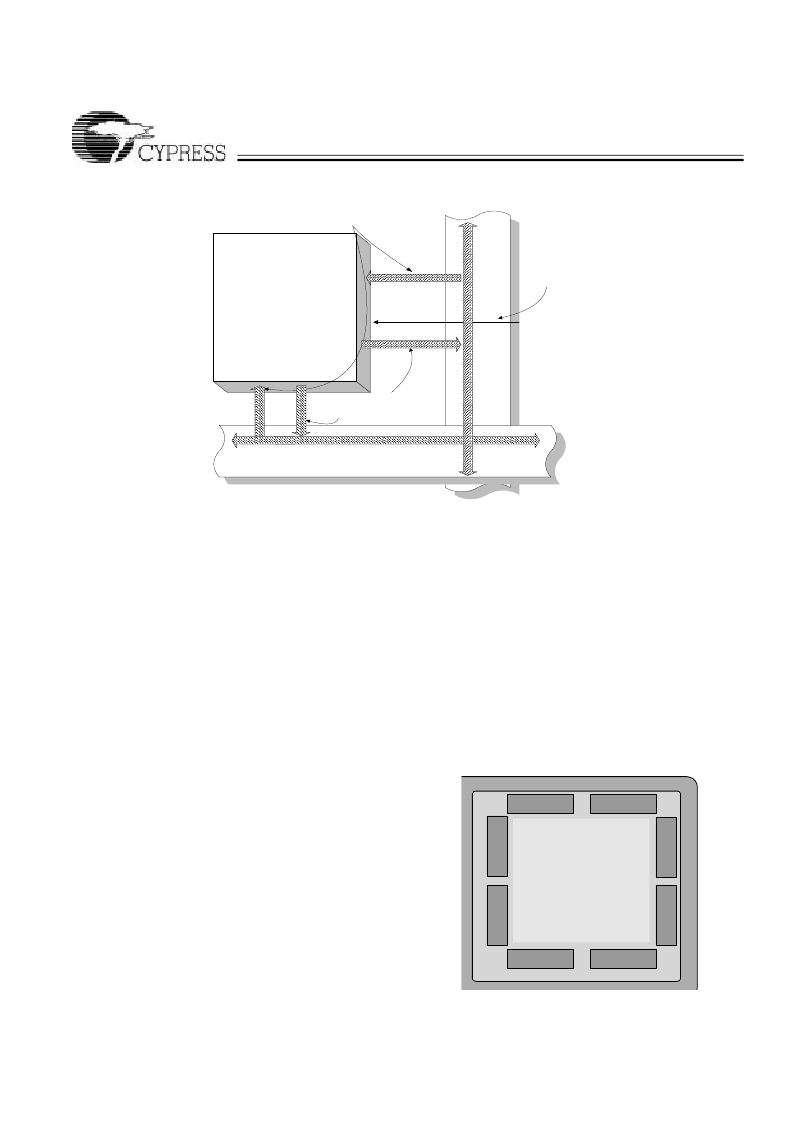
I/O Banks
The Delta39K interfaces the horizontal and vertical routing
channels to the pins through I/O banks. There are eight I/O
banks per device as shown in
Figure 7
, and all I/Os from an
I/O bank are located in the same section of a package for PCB
layout convenience.
Delta39K devices support True Vertical Migration (i.e., for
each package type, Delta39K devices of different densities
keep given pins in the same I/O banks). This allows for easy
and simple implementation of multiple I/O standards during the
design and prototyping phase, before a final density has been
determined. Please refer to the application note titled
“Family,
Package and Density Migration in Delta 39K and Quantum38K
CPLDs.”
Each I/O bank contains several I/O cells, and each I/O cell
contains an input/output register, an output enable register,
programmable slew rate control and programmable bus hold
control logic. Each I/O cell drives a pin output of the device;
the cell also supplies an input to the device that connects to a
dedicated track in the associated routing channel.
Each I/O bank can use any supported I/O standard by
supplying appropriate V
REF
and V
CCIO
voltages and config-
uring the I/O through the Warp software. All the V
REF
and
V
CCIO
pins in an I/O bank must be connected to the same V
REF
and V
CCIO
voltage respectively. This requirement restricts the
number of I/O standards supported by an I/O bank at any given
time.
The number of I/Os which can be used in each I/O bank
depend on the type of I/O standards and the number of V
CCIO
and GND pins being used. This restriction is derived from the
electromigration limit of the V
CCIO
and GND bussing on the
chip. Please refer to the note on page 17 and the application
note titled
“Delta39K Family Device I/O Standards and Config-
urations”
for details.
I/O Cell
Figure 8
is a block diagram of the Delta39K I/O cell. The I/O
cell contains a three-state input buffer, an output buffer, and a
register that can be configured as an input or output register.
The output buffer has a slew rate control option that can be
used to configure the output for a slower slew rate. The input
of the device and the pin output can each be configured as
registered or combinatorial; however, only one path can be
configured as registered in a given design.
The output enable in an I/O cell can be selected from one of
the four global control signals or from one of two Output
Control Channel (OCC) signals. The output enable can be
configured as always enabled or always disabled or it can be
controlled by one of the remaining inputs to the mux. The
selection is done via a mux that includes V
CC
and GND as
inputs.
Figure 6. Block Diagram of Channel Memory Block
4096-bit Dual-Port
Array
Configurable as
Async/Sync Dual-Port
or Sync FIFO
Configurable as
4K x 1, 2K x 2, 1K x 4,
and 512 x 8 block sizes
Horizontal Channel
All channel memory
inputs are driven from
the routing channels
All channel memory outputs
drive dedicated tracks in the
routing channels
GCLK[3:0]
Global Clock
Signals
V
Delta39K
b
b
b
bank 2
bank 3
bank 6
bank 7
Figure 7. Delta39K I/O Bank Block Diagram
相关PDF资料 |
PDF描述 |
|---|---|
| CY39200V388-83BBC | CPLDs at FPGA Densities |
| CY39200V388-83BBI | CPLDs at FPGA Densities |
| CY39200V388-83BGC | CPLDs at FPGA Densities |
| CY39200V388-83BGI | CPLDs at FPGA Densities |
| CY39200V388-83MBC | CPLDs at FPGA Densities |
相关代理商/技术参数 |
参数描述 |
|---|---|
| CY39200V388-83MGC | 制造商:Cypress Semiconductor 功能描述: |
| CY39200V484-125BBC | 制造商:CYPRESS 制造商全称:Cypress Semiconductor 功能描述:CPLDs at FPGA Densities |
| CY39200V484-125BBI | 制造商:CYPRESS 制造商全称:Cypress Semiconductor 功能描述:CPLDs at FPGA Densities |
| CY39200V484-125BBXC | 功能描述:CPLD - 复杂可编程逻辑器件 Delta39K 200K 125MHz COM RoHS:否 制造商:Lattice 系列: 存储类型:EEPROM 大电池数量:128 最大工作频率:333 MHz 延迟时间:2.7 ns 可编程输入/输出端数量:64 工作电源电压:3.3 V 最大工作温度:+ 90 C 最小工作温度:0 C 封装 / 箱体:TQFP-100 |
| CY39200V484-125BBXI | 功能描述:CPLD - 复杂可编程逻辑器件 Delta39K 200K 125MHz IND RoHS:否 制造商:Lattice 系列: 存储类型:EEPROM 大电池数量:128 最大工作频率:333 MHz 延迟时间:2.7 ns 可编程输入/输出端数量:64 工作电源电压:3.3 V 最大工作温度:+ 90 C 最小工作温度:0 C 封装 / 箱体:TQFP-100 |
发布紧急采购,3分钟左右您将得到回复。