- 您现在的位置:买卖IC网 > PDF目录380137 > CY39200V388-83BBC (Cypress Semiconductor Corp.) CPLDs at FPGA Densities PDF资料下载
参数资料
| 型号: | CY39200V388-83BBC |
| 厂商: | Cypress Semiconductor Corp. |
| 英文描述: | CPLDs at FPGA Densities |
| 中文描述: | CPLD器件在FPGA的密度 |
| 文件页数: | 3/86页 |
| 文件大小: | 1235K |
| 代理商: | CY39200V388-83BBC |
第1页第2页当前第3页第4页第5页第6页第7页第8页第9页第10页第11页第12页第13页第14页第15页第16页第17页第18页第19页第20页第21页第22页第23页第24页第25页第26页第27页第28页第29页第30页第31页第32页第33页第34页第35页第36页第37页第38页第39页第40页第41页第42页第43页第44页第45页第46页第47页第48页第49页第50页第51页第52页第53页第54页第55页第56页第57页第58页第59页第60页第61页第62页第63页第64页第65页第66页第67页第68页第69页第70页第71页第72页第73页第74页第75页第76页第77页第78页第79页第80页第81页第82页第83页第84页第85页第86页
Delta39K ISR
CPLD Family
Document #: 38-03039 Rev. *H
Page 3 of 86
General Description
The Delta39K family, based on a 0.18-mm
,
six-layer metal
CMOS logic process, offers a wide range of high-density
solutions at unparalleled system performance. The Delta39K
family is designed to combine the high speed, predictable
timing, and ease of use of CPLDs with the high densities and
low power of FPGAs. With devices ranging from 30,000 to
200,000 usable gates, the family features devices ten times
the size of previously available CPLDs. Even at these large
densities, the Delta39K family is fast enough to implement a
fully synthesizable 64-bit, 66-MHz PCI core.
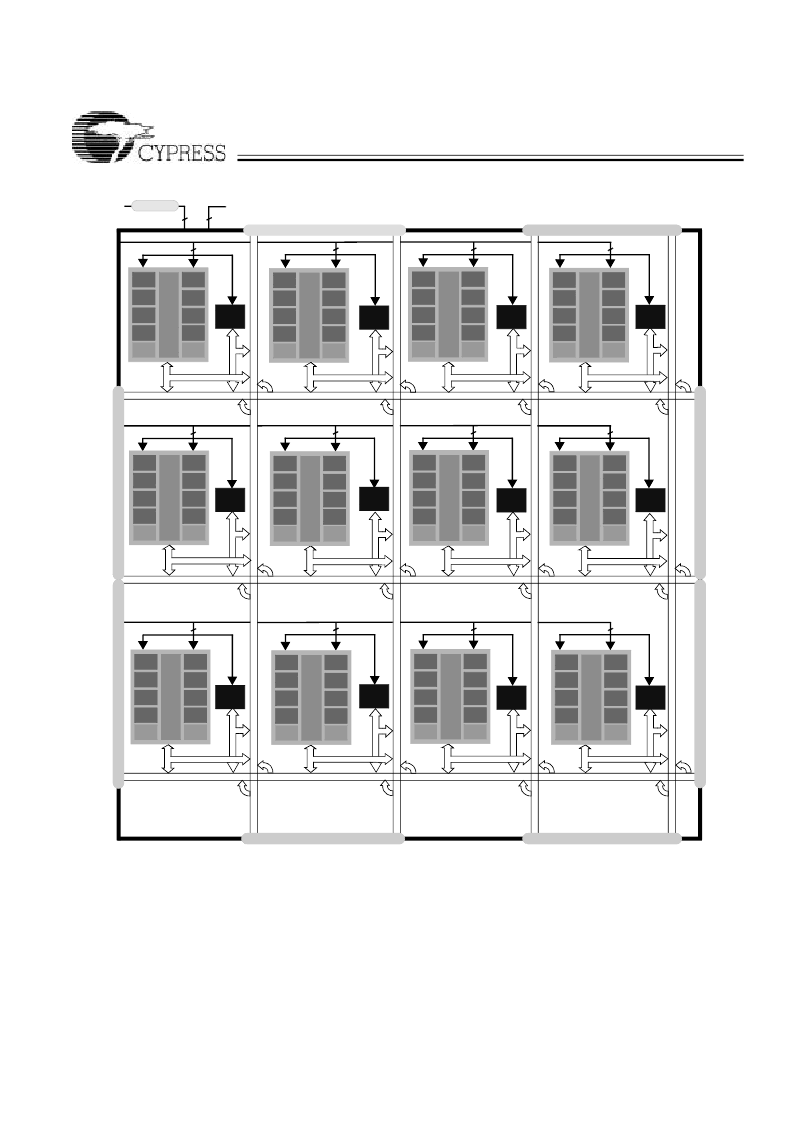
The architecture is based on Logic Block Clusters (LBC) that
are connected by Horizontal and Vertical (H and V) routing
channels. Each LBC features eight individual Logic Blocks
(LB) and two cluster memory blocks. Adjacent to each LBC is
a channel memory block, which can be accessed directly from
the I/O pins. Both types of memory blocks are highly config-
urable and can be cascaded in width and depth. See
Figure 1
for a block diagram of the Delta39K architecture.
All the members of the Delta39K family have Cypress’s highly
regarded In-System Reprogrammability (ISR) feature, which
simplifies both design and manufacturing flows, thereby
reducing costs. The ISR feature provides the ability to recon-
4
GCLK[3:0]
4
4
4
Channel
RAM
4
GCLK[3:0]
4
4
4
4
GCLK[3:0]
4
4
4
4
4
GCLK[3:0]
PLL and Clock MUX
GCTL[3:0]
I/O Bank 6
I/O Bank 7
I/O Bank 3
I/O Bank 2
I
I
I
I
LB 4
LB 3
LB 0
RAM
LB 5
LB 6
LB 7
LB 2
LB 1
PIM
RAM
Channel
RAM
Channel
RAM
Channel
RAM
Channel
RAM
Channel
RAM
Channel
RAM
Channel
RAM
Channel
RAM
Channel
RAM
Channel
RAM
Channel
RAM
LB 4
LB 3
LB 0
Cluster
RAM
LB 5
LB 6
LB 7
LB 2
LB 1
PIM
RAM
LB 4
LB 3
LB 0
Cluster
RAM
LB 5
LB 6
LB 7
LB 2
LB 1
PIM
Cluster
RAM
LB 4
LB 3
LB 0
Cluster
RAM
LB 5
LB 6
LB 7
LB 2
LB 1
PIM
Cluster
RAM
LB 4
LB 3
LB 0
RAM
LB 5
LB 6
LB 7
LB 2
LB 1
PIM
RAM
LB 4
LB 3
LB 0
Cluster
RAM
LB 5
LB 6
LB 7
LB 2
LB 1
PIM
RAM
LB 4
LB 3
LB 0
Cluster
RAM
LB 5
LB 6
LB 7
LB 2
LB 1
PIM
Cluster
RAM
LB 4
LB 3
LB 0
Cluster
RAM
LB 5
LB 6
LB 7
LB 2
LB 1
PIM
Cluster
RAM
LB 4
LB 3
LB 0
Cluster
RAM
LB 5
LB 6
LB 7
LB 2
LB 1
PIM
RAM
LB 4
LB 3
LB 0
Cluster
RAM
LB 5
LB 6
LB 7
LB 2
LB 1
PIM
Cluster
RAM
LB 4
LB 3
LB 0
Cluster
RAM
LB 5
LB 6
LB 7
LB 2
LB 1
PIM
Cluster
RAM
LB 4
LB 3
LB 0
Cluster
RAM
LB 5
LB 6
LB 7
LB 2
LB 1
PIM
RAM
Figure 1. Delta39K100 Block Diagram (Three Rows × Four Columns) with I/O Bank Structure
相关PDF资料 |
PDF描述 |
|---|---|
| CY39200V388-83BBI | CPLDs at FPGA Densities |
| CY39200V388-83BGC | CPLDs at FPGA Densities |
| CY39200V388-83BGI | CPLDs at FPGA Densities |
| CY39200V388-83MBC | CPLDs at FPGA Densities |
| CY39200V388-83MBI | CPLDs at FPGA Densities |
相关代理商/技术参数 |
参数描述 |
|---|---|
| CY39200V388-83MGC | 制造商:Cypress Semiconductor 功能描述: |
| CY39200V484-125BBC | 制造商:CYPRESS 制造商全称:Cypress Semiconductor 功能描述:CPLDs at FPGA Densities |
| CY39200V484-125BBI | 制造商:CYPRESS 制造商全称:Cypress Semiconductor 功能描述:CPLDs at FPGA Densities |
| CY39200V484-125BBXC | 功能描述:CPLD - 复杂可编程逻辑器件 Delta39K 200K 125MHz COM RoHS:否 制造商:Lattice 系列: 存储类型:EEPROM 大电池数量:128 最大工作频率:333 MHz 延迟时间:2.7 ns 可编程输入/输出端数量:64 工作电源电压:3.3 V 最大工作温度:+ 90 C 最小工作温度:0 C 封装 / 箱体:TQFP-100 |
| CY39200V484-125BBXI | 功能描述:CPLD - 复杂可编程逻辑器件 Delta39K 200K 125MHz IND RoHS:否 制造商:Lattice 系列: 存储类型:EEPROM 大电池数量:128 最大工作频率:333 MHz 延迟时间:2.7 ns 可编程输入/输出端数量:64 工作电源电压:3.3 V 最大工作温度:+ 90 C 最小工作温度:0 C 封装 / 箱体:TQFP-100 |
发布紧急采购,3分钟左右您将得到回复。