- 您现在的位置:买卖IC网 > PDF目录380137 > CY39200V388-83BGI (Cypress Semiconductor Corp.) CPLDs at FPGA Densities PDF资料下载
参数资料
| 型号: | CY39200V388-83BGI |
| 厂商: | Cypress Semiconductor Corp. |
| 英文描述: | CPLDs at FPGA Densities |
| 中文描述: | CPLD器件在FPGA的密度 |
| 文件页数: | 22/86页 |
| 文件大小: | 1235K |
| 代理商: | CY39200V388-83BGI |
第1页第2页第3页第4页第5页第6页第7页第8页第9页第10页第11页第12页第13页第14页第15页第16页第17页第18页第19页第20页第21页当前第22页第23页第24页第25页第26页第27页第28页第29页第30页第31页第32页第33页第34页第35页第36页第37页第38页第39页第40页第41页第42页第43页第44页第45页第46页第47页第48页第49页第50页第51页第52页第53页第54页第55页第56页第57页第58页第59页第60页第61页第62页第63页第64页第65页第66页第67页第68页第69页第70页第71页第72页第73页第74页第75页第76页第77页第78页第79页第80页第81页第82页第83页第84页第85页第86页
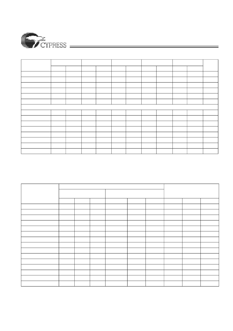
Delta39K ISR
CPLD Family
Document #: 38-03039 Rev. *H
Page 22 of 86
Input and Output Standard Timing Delay
Adjustments
All the timing specifications in this data sheet are specified
based on LVCMOS compliant inputs and outputs (fast slew
rates).
[15]
Apply following adjustments if the inputs and outputs
are configured to operate at other standards.
t
INDUTY
f
PLLO[14]
f
PLLI[14]
f
PLLVCO
P
SAPLLI
f
MPLLI
JTAG Parameters
t
JCKH
t
JCKL
t
JCP
t
JSU
t
JH
t
JCO
t
JXZ
t
JZX
40
6.2
12.5
100
–0.3
60
266
133
266
+0.3
50
40
6.2
12.5
100
–0.3
60
266
133
266
+0.3
50
40
6.2
12.5
100
–0.3
60
266
133
266
+0.3
50
40
6.2
12.5
100
–0.3
60
200
100
266
+0.3
50
40
6.2
12.5
100
–0.3
60
200
100
266
+0.3
50
%
MHz
MHz
MHz
%
KHz
25
25
50
10
10
25
25
50
10
10
25
25
50
10
10
25
25
50
10
10
25
25
50
10
10
ns
ns
ns
ns
ns
ns
ns
ns
20
20
20
20
20
20
20
20
20
20
20
20
20
20
20
Switching Characteristics — Parameter Values
Over the Operating Range (continued)
Parameter
233
200
181
125
83
Unit
Min.
Max.
Min.
Max.
Min.
Max.
Min.
Max.
Min.
Max.
I/O Standard
LVTTL – 2 mA
LVTTL – 4 mA
LVTTL – 6 mA
LVTTL – 8 mA
LVTTL – 12 mA
LVTTL – 16 mA
LVTTL – 24 mA
LVCMOS
LVCMOS3
LVCMOS2
LVCMOS18
3.3V PCI
GTL+
SSTL3 I
SSTL3 II
Output Delay Adjustments
Input Delay Adjustments
t
IOIN
t
CKIN
0
0
0
0
0
0
0
0
0.1
0.1
0.2
0.2
0.5
0.4
0
0.5
0.4
0.5
0.3
0.5
0.3
Fast Slew Rate
t
EA
2.75
1.8
1.8
1.2
0.6
0.16
0
0
0.14
0.05
0.41
1.6
–0.14
0.02
[16]
0.6
[16]
–0.15
–0.4
Slow Slew Rate
(additional delay to fast slew rate)
t
IODSLOW
t
EASLOW
2.6
2.0
2.5
2.0
2.5
2.0
2.4
2.0
2.3
2.0
2.0
2.0
1.6
2.0
2.0
2.0
2.0
2.0
2.0
2.0
2.1
2.0
2.0
2.0
2.0
2.0
2.0
2.0
2.0
2.0
t
IOD
t
ER
t
ERSLOW
2.0
2.0
2.0
2.0
2.0
2.0
2.0
2.0
2.0
2.0
2.0
2.0
2.0
2.0
2.0
t
IOREGPIN
0
0
0
0
0
0
0
0
0.2
0.4
0.3
0
0.2
0.3
0.3
0
0
0
0
0
0
0
0
0
0
0
0
0
0
0
0
0
0
0
0
0
0
0
0
0
0
0.1
0.7
0
0.1
0
0.9
[16]
0.1
0
0
0.3
0.2
Notes:
14. Refer to page 11 and the application note titled
“Delta39K PLL and Clock Tree”
for details on the PLL operation.
15. For “slow slew rate” output delay adjustments, refer to
Warp
software’s static timing analyzer results.
16. These delays are based on falling edge output. The rising edge delay depends on the size of pull-up resistor and termination voltage.
相关PDF资料 |
PDF描述 |
|---|---|
| CY39200V388-83MBC | CPLDs at FPGA Densities |
| CY39200V388-83MBI | CPLDs at FPGA Densities |
| CY39050Z484-83MGC | CPLDs at FPGA Densities |
| CY39050Z484-83MGI | CPLDs at FPGA Densities |
| CY39050Z484-83NC | CPLDs at FPGA Densities |
相关代理商/技术参数 |
参数描述 |
|---|---|
| CY39200V388-83MGC | 制造商:Cypress Semiconductor 功能描述: |
| CY39200V484-125BBC | 制造商:CYPRESS 制造商全称:Cypress Semiconductor 功能描述:CPLDs at FPGA Densities |
| CY39200V484-125BBI | 制造商:CYPRESS 制造商全称:Cypress Semiconductor 功能描述:CPLDs at FPGA Densities |
| CY39200V484-125BBXC | 功能描述:CPLD - 复杂可编程逻辑器件 Delta39K 200K 125MHz COM RoHS:否 制造商:Lattice 系列: 存储类型:EEPROM 大电池数量:128 最大工作频率:333 MHz 延迟时间:2.7 ns 可编程输入/输出端数量:64 工作电源电压:3.3 V 最大工作温度:+ 90 C 最小工作温度:0 C 封装 / 箱体:TQFP-100 |
| CY39200V484-125BBXI | 功能描述:CPLD - 复杂可编程逻辑器件 Delta39K 200K 125MHz IND RoHS:否 制造商:Lattice 系列: 存储类型:EEPROM 大电池数量:128 最大工作频率:333 MHz 延迟时间:2.7 ns 可编程输入/输出端数量:64 工作电源电压:3.3 V 最大工作温度:+ 90 C 最小工作温度:0 C 封装 / 箱体:TQFP-100 |
发布紧急采购,3分钟左右您将得到回复。