- 您现在的位置:买卖IC网 > PDF目录295373 > CY7C1157V18-333BZXC (CYPRESS SEMICONDUCTOR CORP) 18-Mbit DDR-II+ SRAM 2-Word Burst Architecture (2.0 Cycle Read Latency) PDF资料下载
参数资料
| 型号: | CY7C1157V18-333BZXC |
| 厂商: | CYPRESS SEMICONDUCTOR CORP |
| 元件分类: | SRAM |
| 英文描述: | 18-Mbit DDR-II+ SRAM 2-Word Burst Architecture (2.0 Cycle Read Latency) |
| 中文描述: | 2M X 9 DDR SRAM, 0.45 ns, PBGA165 |
| 封装: | 13 X 15 MM, 1.40 MM HEIGHT, LEAD FREE, MO-216, FBGA-165 |
| 文件页数: | 3/27页 |
| 文件大小: | 645K |
| 代理商: | CY7C1157V18-333BZXC |
第1页第2页当前第3页第4页第5页第6页第7页第8页第9页第10页第11页第12页第13页第14页第15页第16页第17页第18页第19页第20页第21页第22页第23页第24页第25页第26页第27页
CY7C1146V18, CY7C1157V18
CY7C1148V18, CY7C1150V18
Document Number: 001-06621 Rev. *D
Page 11 of 27
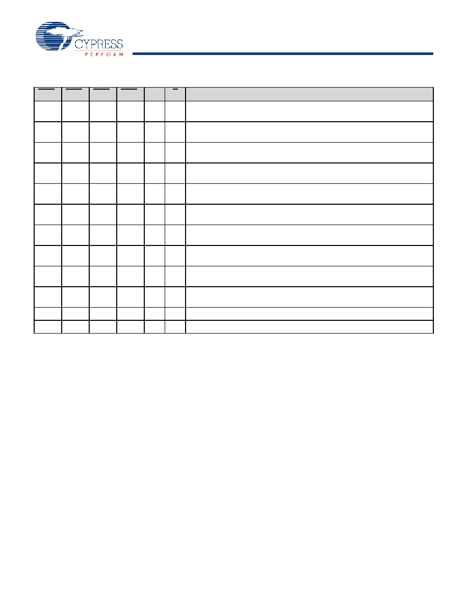
BWS0
BWS1
BWS2
BWS3
K
Comments
LLLL
L – H
–
When the Data portion of a write sequence is active, all four bytes (D[35:0]) are
written into the device.
LLLL
–
L – H When the Data portion of a write sequence is active, all four bytes (D[35:0]) are
written into the device.
L
H
L – H
–
When the Data portion of a write sequence is active, only the lower byte (D[8:0]) is
written into the device. D[35:9] remains unaltered.
L
H
–
L – H When the Data portion of a write sequence is active, only the lower byte (D[8:0]) is
written into the device. D[35:9] remains unaltered.
H
L
H
L – H
–
When the Data portion of a write sequence is active, only the byte (D[17:9]) is written
into the device. D[8:0] and D[35:18] remains unaltered.
H
L
H
–
L – H When the Data portion of a write sequence is active, only the byte (D[17:9]) is written
into the device. D[8:0] and D[35:18] remains unaltered.
H
L
H
L – H
–
When the Data portion of a write sequence is active, only the byte (D[26:18]) is
written into the device. D[17:0] and D[35:27] remains unaltered.
H
L
H
–
L – H When the Data portion of a Write sequence is active, only the byte (D[26:18]) is
written into the device. D[17:0] and D[35:27] remains unaltered.
H
L
L – H
–
When the Data portion of a write sequence is active, only the byte (D[35:27]) is
written into the device. D[26:0] remains unaltered.
H
L
–
L – H When the Data portion of a write sequence is active, only the byte (D[35:27]) is
written into the device. D[26:0] remains unaltered.
HHHH
L – H
–
No data is written into the device when this portion of a write operation is active.
HHHH
–
L – H No data is written into the device when this portion of a write operation is active.
相关PDF资料 |
PDF描述 |
|---|---|
| CY7C1157V18-333BZXI | 18-Mbit DDR-II+ SRAM 2-Word Burst Architecture (2.0 Cycle Read Latency) |
| CY7C1157V18-375BZC | 18-Mbit DDR-II+ SRAM 2-Word Burst Architecture (2.0 Cycle Read Latency) |
| CY7C1157V18-375BZI | 18-Mbit DDR-II+ SRAM 2-Word Burst Architecture (2.0 Cycle Read Latency) |
| CY7C1157V18-375BZXC | 18-Mbit DDR-II+ SRAM 2-Word Burst Architecture (2.0 Cycle Read Latency) |
| CY7C1157V18-375BZXI | 18-Mbit DDR-II+ SRAM 2-Word Burst Architecture (2.0 Cycle Read Latency) |
相关代理商/技术参数 |
参数描述 |
|---|---|
| CY7C1163KV18-400BZI | 功能描述:静态随机存取存储器 18MB (1Mx18) 1.8v 400MHz DDR II 静态随机存取存储器 RoHS:否 制造商:Cypress Semiconductor 存储容量:16 Mbit 组织:1 M x 16 访问时间:55 ns 电源电压-最大:3.6 V 电源电压-最小:2.2 V 最大工作电流:22 uA 最大工作温度:+ 85 C 最小工作温度:- 40 C 安装风格:SMD/SMT 封装 / 箱体:TSOP-48 封装:Tray |
| CY7C1163KV18-450BZC | 功能描述:静态随机存取存储器 18MB (1Mx18) 1.8v 450MHz DDR II 静态随机存取存储器 RoHS:否 制造商:Cypress Semiconductor 存储容量:16 Mbit 组织:1 M x 16 访问时间:55 ns 电源电压-最大:3.6 V 电源电压-最小:2.2 V 最大工作电流:22 uA 最大工作温度:+ 85 C 最小工作温度:- 40 C 安装风格:SMD/SMT 封装 / 箱体:TSOP-48 封装:Tray |
| CY7C1163KV18-550BZC | 功能描述:静态随机存取存储器 18MB (1Mx18) 1.8v 550MHz DDR II 静态随机存取存储器 RoHS:否 制造商:Cypress Semiconductor 存储容量:16 Mbit 组织:1 M x 16 访问时间:55 ns 电源电压-最大:3.6 V 电源电压-最小:2.2 V 最大工作电流:22 uA 最大工作温度:+ 85 C 最小工作温度:- 40 C 安装风格:SMD/SMT 封装 / 箱体:TSOP-48 封装:Tray |
| CY7C11651KV18-400BZC | 功能描述:静态随机存取存储器 Sync 静态随机存取存储器 QDR RoHS:否 制造商:Cypress Semiconductor 存储容量:16 Mbit 组织:1 M x 16 访问时间:55 ns 电源电压-最大:3.6 V 电源电压-最小:2.2 V 最大工作电流:22 uA 最大工作温度:+ 85 C 最小工作温度:- 40 C 安装风格:SMD/SMT 封装 / 箱体:TSOP-48 封装:Tray |
| CY7C11651KV18-400BZXC | 功能描述:IC SRAM 18MBIT 400MHZ 165-FPBGA RoHS:是 类别:集成电路 (IC) >> 存储器 系列:- 标准包装:150 系列:- 格式 - 存储器:EEPROMs - 串行 存储器类型:EEPROM 存储容量:4K (2 x 256 x 8) 速度:400kHz 接口:I²C,2 线串口 电源电压:2.5 V ~ 5.5 V 工作温度:-40°C ~ 85°C 封装/外壳:8-VFDFN 裸露焊盘 供应商设备封装:8-DFN(2x3) 包装:管件 产品目录页面:1445 (CN2011-ZH PDF) |
发布紧急采购,3分钟左右您将得到回复。