- 您现在的位置:买卖IC网 > PDF目录380191 > CY7C1352-100AC (CYPRESS SEMICONDUCTOR CORP) 256K x18 Pipelined SRAM with NoBL Architecture PDF资料下载
参数资料
| 型号: | CY7C1352-100AC |
| 厂商: | CYPRESS SEMICONDUCTOR CORP |
| 元件分类: | DRAM |
| 英文描述: | 256K x18 Pipelined SRAM with NoBL Architecture |
| 中文描述: | 256K X 18 ZBT SRAM, 5 ns, PQFP100 |
| 封装: | 14 X 20 MM, 1.40 MM HEIGHT, PLASTIC, TQFP-100 |
| 文件页数: | 3/12页 |
| 文件大小: | 197K |
| 代理商: | CY7C1352-100AC |
CY7C1352
3
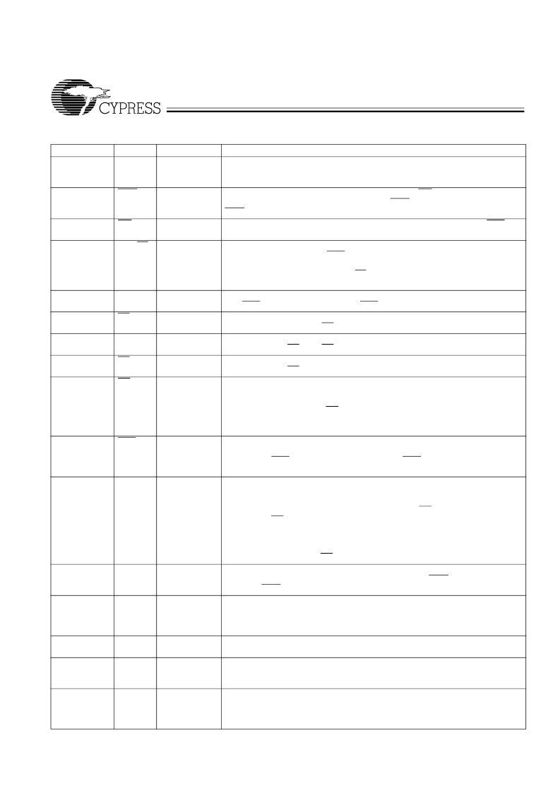
Pin Definitions
Pin Number
80, 50
44,
81
82, 99
100, 32
37
94, 93
Name
A
[17:0]
I/O
Input-
Description
Synchronous
Address Inputs used to select one of the 262,144 address locations. Sampled at
the rising edge of the CLK.
BWS
[1:0]
Input-
Synchronous
Byte Write Select Inputs, active LOW. Qualified with WE to conduct writes to the
SRAM. Sampled on the rising edge of CLK. BWS
0
controls DQ
[7:0]
and DP
0
,
BWS
1
controls DQ
[15:8]
and DP
1
. See Write Cycle Description table for details.
Write Enable Input, active LOW. Sampled on the rising edge of CLK if CEN is
active LOW. This signal must be asserted LOW to initiate a write sequence.
Advance/Load input used to advance the on-chip address counter or load a new
address. When HIGH (and CEN is asserted LOW) the internal burst counter is
advanced. When LOW, a new address can be loaded into the device for an ac-
cess. After being deselected, ADV/LD should be driven LOW in order to load a
new address.
Clock input. Used to capture all synchronous inputs to the device. CLK is qualified
with CEN. CLK is only recognized if CEN is active LOW.
Chip Enable 1 Input active LOW. Sampled on the rising edge of CLK. Used in
conjunction with CE
2
and CE
3
to select/deselect the device.
Chip Enable 2 Input active HIGH. Sampled on the rising edge of CLK. Used in
conjunction with CE
1
and CE
3
to select/deselect the device.
Chip Enable 3 Input, active LOW. Sampled on the rising edge of CLK. Used in
conjunction with CE
1
and
CE
2
to select/deselect the device.
Output Enable, active LOW. Combined with the synchronous logic block inside
the device to control the direction of the I/O pins. When LOW, the I/O pins are
allowed to behave as outputs. When deasserted HIGH, I/O pins are three-stated,
and act as input data pins. OE is masked during the data portion of a write
sequence, during the first clock when emerging from a deselected state, when
the device has been deselected.
Clock Enable Input, active LOW. When asserted LOW the clock signal is recog-
nized by the SRAM. When deasserted HIGH the Clock signal is masked. Since
deasserting CEN does not deselect the device, CEN can be used to extend the
previous cycle when required.
Bidirectional Data I/O lines. As inputs, they feed into an on-chip data register that
is triggered by the rising edge of CLK. As outputs, they deliver the data contained
in the memory location specified by A
[16:0]
during the previous clock rise of the
read cycle. The direction of the pins is controlled by OE and the internal control
logic. When OE is asserted LOW, the pins can behave as outputs. When HIGH,
DQ
[15:0]
are placed in a three-state condition. The outputs are automatically
three-stated during the data portion of a write sequence, during the first clock
when emerging from a deselected state, and when the device is deselected,
regardless of the state of OE.
Bidirectional Data Parity I/O lines. Functionally, these signals are identical to
DQ
[15:0]
. During write sequences, DP
0
is controlled by BWS
0
and DP
1
is con-
trolled by BWS
1
Mode input. Selects the burst order of the device. Tied HIGH selects the inter-
leaved burst order. Pulled LOW selects the linear burst order. MODE should not
change states during operation. When left floating, MODE will default HIGH to an
interleaved burst order.
Power supply inputs to the core of the device. Should be connected to 3.3V power
supply.
Power supply for the I/O circuitry. Should be connected to a 3.3V power supply.
88
WE
Input-
Synchronous
Input-
Synchronous
85
ADV/LD
89
CLK
Input-Clock
98
CE
1
Input-
Synchronous
Input-
Synchronous
Input-
Synchronous
Input-
Asynchronous
97
CE
2
92
CE
3
86
OE
87
CEN
Input-
Synchronous
23
22, 19
18,
13
12, 9
8,
73
72, 69
68,
63
62, 59
58
DQ
[15:0]
I/O-
Synchronous
24, 74
DP
[1:0]
I/O-
Synchronous
31
MODE
Input
Strap pin
15, 16, 41, 65,
66, 91
4, 11, 14, 20,
27, 54, 61, 70,
77
5, 10, 17, 21,
26, 40, 55, 60,
64, 67, 71, 76,
90
V
DD
Power Supply
V
DDQ
I/O Power
Supply
V
SS
Ground
Ground for the device. Should be connected to ground of the system.
相关PDF资料 |
PDF描述 |
|---|---|
| CY7C1352-133AC | 256K x18 Pipelined SRAM with NoBL Architecture |
| CY7C1352-80AC | 256K x18 Pipelined SRAM with NoBL Architecture |
| CY7C1352F | CTV 99C 97#22D 2#8(TWINAX) SKT |
| CY7C1352F-100AC | 4-Mbit (256Kx18) Pipelined SRAM with NoBL⑩ Architecture |
| CY7C1352F-100AI | 4-Mbit (256Kx18) Pipelined SRAM with NoBL⑩ Architecture |
相关代理商/技术参数 |
参数描述 |
|---|---|
| CY7C135-25JC | 制造商:Cypress Semiconductor 功能描述:SRAM Chip Async Dual 5V 32K-Bit 4K x 8 25ns 52-Pin PLCC 制造商:Rochester Electronics LLC 功能描述:4KX8 52PIN CMOS DUAL PORT SRAM - Bulk |
| CY7C135-25JXC | 功能描述:IC SRAM 32KBIT 25NS 52PLCC RoHS:是 类别:集成电路 (IC) >> 存储器 系列:- 标准包装:1,000 系列:- 格式 - 存储器:RAM 存储器类型:移动 SDRAM 存储容量:256M(8Mx32) 速度:133MHz 接口:并联 电源电压:1.7 V ~ 1.95 V 工作温度:-40°C ~ 85°C 封装/外壳:90-VFBGA 供应商设备封装:90-VFBGA(8x13) 包装:带卷 (TR) 其它名称:557-1327-2 |
| CY7C135-25JXI | 功能描述:静态随机存取存储器 4Kx8 32Kb 25ns DUAL PORT 静态随机存取存储器 RoHS:否 制造商:Cypress Semiconductor 存储容量:16 Mbit 组织:1 M x 16 访问时间:55 ns 电源电压-最大:3.6 V 电源电压-最小:2.2 V 最大工作电流:22 uA 最大工作温度:+ 85 C 最小工作温度:- 40 C 安装风格:SMD/SMT 封装 / 箱体:TSOP-48 封装:Tray |
| CY7C1352B100AC | 制造商:Cypress Semiconductor 功能描述: |
| CY7C1352B-100AC | 制造商:Cypress Semiconductor 功能描述:SRAM Chip Sync Single 3.3V 4.5M-Bit 256K x 18 5ns 100-Pin TQFP |
发布紧急采购,3分钟左右您将得到回复。