- 您现在的位置:买卖IC网 > PDF目录295374 > CY7C1387DV25-225BZC (CYPRESS SEMICONDUCTOR CORP) 1M X 18 CACHE SRAM, 2.8 ns, PBGA165 PDF资料下载
参数资料
| 型号: | CY7C1387DV25-225BZC |
| 厂商: | CYPRESS SEMICONDUCTOR CORP |
| 元件分类: | SRAM |
| 英文描述: | 1M X 18 CACHE SRAM, 2.8 ns, PBGA165 |
| 封装: | 13 X 15 MM, 1.40 MM HEIGHT, FBGA-165 |
| 文件页数: | 16/32页 |
| 文件大小: | 501K |
| 代理商: | CY7C1387DV25-225BZC |
第1页第2页第3页第4页第5页第6页第7页第8页第9页第10页第11页第12页第13页第14页第15页当前第16页第17页第18页第19页第20页第21页第22页第23页第24页第25页第26页第27页第28页第29页第30页第31页第32页
PRELIMINARY
CY7C1386DV25
CY7C1387DV25
Document #: 38-05548 Rev. **
Page 23 of 32
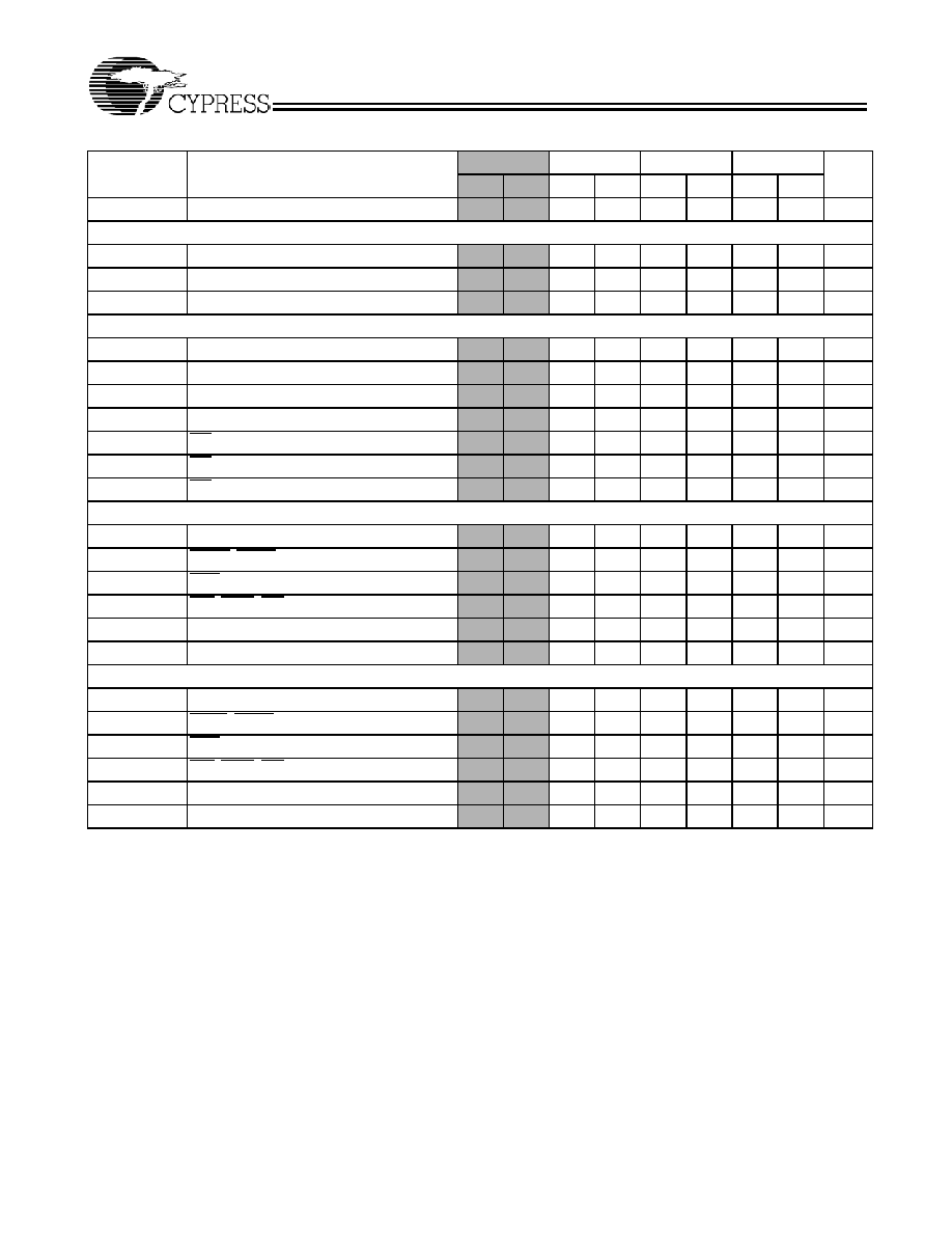
Switching Characteristics Over the Operating Range[20, 21]
Parameter
Description
250 MHz
225 MHz
200 MHz
167 MHz
Unit
Min.
Max.
Min.
Max.
Min.
Max.
Min.
Max.
tPOWER
VDD(Typical) to the first Access[16]
1
11
ms
Clock
tCYC
Clock Cycle Time
4.0
4.4
5.0
6.0
ns
tCH
Clock HIGH
1.7
2.0
2.2
ns
tCL
Clock LOW
1.7
2.0
2.2
ns
Output Times
tCO
Data Output Valid After CLK Rise
2.6
2.8
3.0
3.4
ns
tDOH
Data Output Hold After CLK Rise
1.0
1.3
ns
tCLZ
Clock to Low-Z[17, 18, 19]
1.0
1.3
ns
tCHZ
Clock to High-Z[17, 18, 19]
2.6
2.8
3.0
3.4
ns
tOEV
OE LOW to Output Valid
2.6
2.8
3.0
3.4
ns
tOELZ
OE LOW to Output Low-Z[17, 18, 19]
0
ns
tOEHZ
OE HIGH to Output High-Z[17, 18, 19]
2.6
2.8
3.0
3.4
ns
Setup Times
tAS
Address Set-up Before CLK Rise
1.2
1.4
1.5
ns
tADS
ADSC, ADSP Set-up Before CLK Rise
1.2
1.4
1.5
ns
tADVS
ADV Set-up Before CLK Rise
1.2
1.4
1.5
ns
tWES
GW, BWE, BWX Set-up Before CLK Rise
1.2
1.4
1.5
ns
tDS
Data Input Set-up Before CLK Rise
1.2
1.4
1.5
ns
tCES
Chip Enable Set-Up Before CLK Rise
1.2
1.4
1.5
ns
Hold Times
tAH
Address Hold After CLK Rise
0.3
0.4
0.5
ns
tADH
ADSP, ADSC Hold After CLK Rise
0.3
0.4
0.5
ns
tADVH
ADV Hold After CLK Rise
0.3
0.4
0.5
ns
tWEH
GW, BWE, BWX Hold After CLK Rise
0.3
0.4
0.5
ns
tDH
Data Input Hold After CLK Rise
0.3
0.4
0.5
ns
tCEH
Chip Enable Hold After CLK Rise
0.3
0.4
0.5
ns
Shaded areas contain advance information.
Notes:
16. This part has a voltage regulator internally; tPOWER is the time that the power needs to be supplied above VDD(minimum) initially before a read or write operation
can be initiated.
17. tCHZ, tCLZ,tOELZ, and tOEHZ are specified with AC test conditions shown in part (b) of AC Test Loads. Transition is measured ± 200 mV from steady-state voltage.
18. At any given voltage and temperature, tOEHZ is less than tOELZ and tCHZ is less than tCLZ to eliminate bus contention between SRAMs when sharing the same
data bus. These specifications do not imply a bus contention condition, but reflect parameters guaranteed over worst case user conditions. Device is designed
to achieve High-Z prior to Low-Z under the same system conditions
19. This parameter is sampled and not 100% tested.
20. Timing reference level is 1.25V when VDDQ = 2.5V.
21. Test conditions shown in (a) of AC Test Loads unless otherwise noted.
相关PDF资料 |
PDF描述 |
|---|---|
| CY7C138AV | Memory |
| CY7C025-15JC | x16 Dual-Port SRAM |
| CY7C0251AV-20AC | x18 Dual-Port SRAM |
| CY7C0251AV-25AC | x18 Dual-Port SRAM |
| CY7C025-25AC | x16 Dual-Port SRAM |
相关代理商/技术参数 |
参数描述 |
|---|---|
| CY7C138XC | 制造商:Cypress Semiconductor 功能描述: |
| CY7C139-25JC | 制造商:Cypress Semiconductor 功能描述: |
| CY7C139-25JXC | 功能描述:IC SRAM 36KBIT 25NS 68PLCC RoHS:是 类别:集成电路 (IC) >> 存储器 系列:- 标准包装:1,000 系列:- 格式 - 存储器:RAM 存储器类型:移动 SDRAM 存储容量:256M(8Mx32) 速度:133MHz 接口:并联 电源电压:1.7 V ~ 1.95 V 工作温度:-40°C ~ 85°C 封装/外壳:90-VFBGA 供应商设备封装:90-VFBGA(8x13) 包装:带卷 (TR) 其它名称:557-1327-2 |
| CY7C1392CV18-200BZC | 功能描述:静态随机存取存储器 2Mx8 1.8V DDR II SIO 静态随机存取存储器 RoHS:否 制造商:Cypress Semiconductor 存储容量:16 Mbit 组织:1 M x 16 访问时间:55 ns 电源电压-最大:3.6 V 电源电压-最小:2.2 V 最大工作电流:22 uA 最大工作温度:+ 85 C 最小工作温度:- 40 C 安装风格:SMD/SMT 封装 / 箱体:TSOP-48 封装:Tray |
| CY7C1392CV18-250BZC | 功能描述:静态随机存取存储器 2Mx8 1.8V DDR II SIO 静态随机存取存储器 RoHS:否 制造商:Cypress Semiconductor 存储容量:16 Mbit 组织:1 M x 16 访问时间:55 ns 电源电压-最大:3.6 V 电源电压-最小:2.2 V 最大工作电流:22 uA 最大工作温度:+ 85 C 最小工作温度:- 40 C 安装风格:SMD/SMT 封装 / 箱体:TSOP-48 封装:Tray |
发布紧急采购,3分钟左右您将得到回复。