- 您现在的位置:买卖IC网 > PDF目录295362 > CY7C1399V-12ZC x8 SRAM PDF资料下载
参数资料
| 型号: | CY7C1399V-12ZC |
| 英文描述: | x8 SRAM |
| 中文描述: | x8的SRAM |
| 文件页数: | 3/9页 |
| 文件大小: | 194K |
| 代理商: | CY7C1399V-12ZC |
CY7C1019B/
CY7C10191B
Document #: 38-05026 Rev. *A
Page 3 of 9
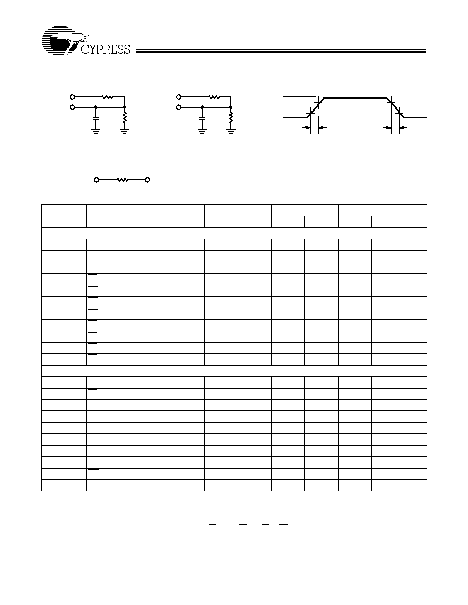
AC Test Loads and Waveforms
Switching Characteristics[4] Over the Operating Range
7C10191B-10
7C1019B-12
7C1019B-15
Parameter
Description
Min.Max.Min.Max.Min.Max.
Unit
Read Cycle
tRC
Read Cycle Time
10
12
15
ns
tAA
Address to Data Valid
10
12
15
ns
tOHA
Data Hold from Address Change
3
ns
tACE
CE LOW to Data Valid
101215
ns
tDOE
OE LOW to Data Valid
5
6
7
ns
tLZOE
OE LOW to Low Z
0
ns
tHZOE
OE HIGH to High Z[5, 6]
56
7
ns
tLZCE
CE LOW to Low Z[6]
33
3
ns
tHZCE
CE HIGH to High Z[5, 6]
56
7
ns
tPU
CE LOW to Power-Up
0
ns
tPD
CE HIGH to Power-Down
10
12
15
ns
Write Cycle[7, 8]
tWC
Write Cycle Time
10
12
15
ns
tSCE
CE LOW to Write End
8
9
10
ns
tAW
Address Set-Up to Write End
7
8
10
ns
tHA
Address Hold from Write End
0
ns
tSA
Address Set-Up to Write Start
0
ns
tPWE
WE Pulse Width
7
8
10
ns
tSD
Data Set-Up to Write End
5
6
8
ns
tHD
Data Hold from Write End
0
ns
tLZWE
WE HIGH to Low Z[6]
33
3
ns
tHZWE
WE LOW to High Z[5, 6]
56
7
ns
Notes:
4.
Test conditions assume signal transition time of 3 ns or less, timing reference levels of 1.5V, input pulse levels of 0 to 3.0V, and output loading of the specified
IOL/IOH and 30-pF load capacitance.
5.
tHZOE, tHZCE, and tHZWE are specified with a load capacitance of 5 pF as in part (b) of AC Test Loads. Transition is measured ±500 mV from steady-state voltage.
6.
At any given temperature and voltage condition, tHZCE is less than tLZCE, tHZOE is less than tLZOE, and tHZWE is less than tLZWE for any given device.
7.
The internal write time of the memory is defined by the overlap of CE LOW and WE LOW. CE and WE must be LOW to initiate a write, and the transition of any of these
signals can terminate the write. The input data set-up and hold timing should be referenced to the leading edge of the signal that terminates the write.
8.
The minimum write cycle time for Write Cycle no. 3 (WE controlled, OE LOW) is the sum of tHZWE and tSD.
90%
10%
3.0V
GND
90%
10%
ALL INPUT PULSES
5V
OUTPUT
30 pF
INCLUDING
JIG AND
SCOPE
5V
OUTPUT
5 pF
INCLUDING
JIG AND
SCOPE
(a)
(b)
≤ 3 ns
OUTPUT
R1 480
R1 480
R2
255
R2
255
167
Equivalent to:
VENIN EQUIVALENT
1.73V
TH
相关PDF资料 |
PDF描述 |
|---|---|
| CY7C1399V-15ZI | x8 SRAM |
| CY7C1399V-20VC | x8 SRAM |
| CY7C1399V-20ZC | x8 SRAM |
| CY7C1399V-25VC | x8 SRAM |
| CY7C1399V-25ZC | x8 SRAM |
相关代理商/技术参数 |
参数描述 |
|---|---|
| CY7C140 WAF | 制造商:Cypress Semiconductor 功能描述: |
| CY7C140-35DMB | 制造商:Rochester Electronics LLC 功能描述:- Bulk |
| CY7C140-45DMB | 制造商:Rochester Electronics LLC 功能描述:- Bulk |
| CY7C1411BV18-250BZC | 功能描述:静态随机存取存储器 1Mx36 QDR II Burst 4 静态随机存取存储器 RoHS:否 制造商:Cypress Semiconductor 存储容量:16 Mbit 组织:1 M x 16 访问时间:55 ns 电源电压-最大:3.6 V 电源电压-最小:2.2 V 最大工作电流:22 uA 最大工作温度:+ 85 C 最小工作温度:- 40 C 安装风格:SMD/SMT 封装 / 箱体:TSOP-48 封装:Tray |
| CY7C1411KV18-250BZC | 功能描述:静态随机存取存储器 36Mb QDR II 静态随机存取存储器 RoHS:否 制造商:Cypress Semiconductor 存储容量:16 Mbit 组织:1 M x 16 访问时间:55 ns 电源电压-最大:3.6 V 电源电压-最小:2.2 V 最大工作电流:22 uA 最大工作温度:+ 85 C 最小工作温度:- 40 C 安装风格:SMD/SMT 封装 / 箱体:TSOP-48 封装:Tray |
发布紧急采购,3分钟左右您将得到回复。