- 您现在的位置:买卖IC网 > PDF目录378509 > CY7C1481V25-133AXI (CYPRESS SEMICONDUCTOR CORP) 72-Mbit (2M x 36/4M x 18/1M x 72) Flow-Through SRAM PDF资料下载
参数资料
| 型号: | CY7C1481V25-133AXI |
| 厂商: | CYPRESS SEMICONDUCTOR CORP |
| 元件分类: | DRAM |
| 英文描述: | 72-Mbit (2M x 36/4M x 18/1M x 72) Flow-Through SRAM |
| 中文描述: | 2M X 36 CACHE SRAM, 6.5 ns, PQFP100 |
| 封装: | 14 X 20 MM, 1.40 MM HEIGHT, LEAD FREE, PLASTIC, MS-026, TQFP-100 |
| 文件页数: | 12/30页 |
| 文件大小: | 1028K |
| 代理商: | CY7C1481V25-133AXI |
第1页第2页第3页第4页第5页第6页第7页第8页第9页第10页第11页当前第12页第13页第14页第15页第16页第17页第18页第19页第20页第21页第22页第23页第24页第25页第26页第27页第28页第29页第30页
CY7C1481V25
CY7C1483V25
CY7C1487V25
Document #: 38-05281 Rev. *H
Page 12 of 30
IEEE 1149.1 Serial Boundary Scan (JTAG)
The CY7C1481V25/CY7C1483V25/CY7C1487V25 incorpo-
rates a serial boundary scan test access port (TAP). This port
operates in accordance with IEEE Standard 1149.1-1990 but
does not have the set of functions required for full 1149.1
compliance. These functions from the IEEE specification are
excluded because their inclusion places an added delay in the
critical speed path of the SRAM. Note that the TAP controller
functions in a manner that does not conflict with the operation
of other devices using 1149.1 fully compliant TAPs. The TAP
operates using JEDEC-standard 2.5V or 1.8V I/O logic levels.
The CY7C1481V25/CY7C1483V25 contains a TAP controller,
instruction register, boundary scan register, bypass register,
and ID register.
Disabling the JTAG Feature
It is possible to operate the SRAM without using the JTAG
feature. To disable the TAP controller, tie TCK LOW (V
SS
) to
prevent device clocking. TDI and TMS are internally pulled up
and may be unconnected. They may alternatively be
connected to V
DD
through a pull up resistor. TDO should be
left unconnected. Upon power up, the device comes up in a
reset state that does not interfere with the operation of the
device.
The 0/1 next to each state represents the value of TMS at the
rising edge of TCK.
Test Access Port (TAP)
Test Clock (TCK)
The test clock is used only with the TAP controller. All inputs
are captured on the rising edge of TCK. All outputs are driven
from the falling edge of TCK.
Test MODE SELECT (TMS)
The TMS input gives commands to the TAP controller and is
sampled on the rising edge of TCK. You can leave this ball
unconnected if the TAP is not used. The ball is pulled up inter-
nally, resulting in a logic HIGH level.
Test Data-In (TDI)
The TDI ball serially inputs information into the registers and
can be connected to the input of any of the registers. The
register between TDI and TDO is chosen by the instruction
that is loaded into the TAP instruction register. For information
on loading the instruction register, see the
TAP Controller
State Diagram
. TDI is internally pulled up and can be uncon-
nected if the TAP is unused in an application. TDI is connected
to the most significant bit (MSB) of any register. (See
TAP
Controller Block Diagram
.)
Test Data-Out (TDO)
The TDO output ball is used to serially clock data-out from the
registers. The output is active depending upon the current
state of the TAP state machine. The output changes on the
falling edge of TCK. TDO is connected to the least significant
bit (LSB) of any register. (See
TAP Controller State Diagram
.)
Performing a TAP Reset
To perform a RESET, force TMS HIGH (V
DD
) for five rising
edges of TCK. This RESET does not affect the operation of
the SRAM and may be performed while the SRAM is
operating.
At power up, the TAP is reset internally to ensure that TDO
comes up in a High-Z state.
TAP Registers
Registers are connected between the TDI and TDO balls and
enable data to be scanned into and out of the SRAM test
circuitry. Only one register can be selected at a time through
the instruction register. Data is serially loaded into the TDI ball
on the rising edge of TCK. Data is output on the TDO ball on
the falling edge of TCK.
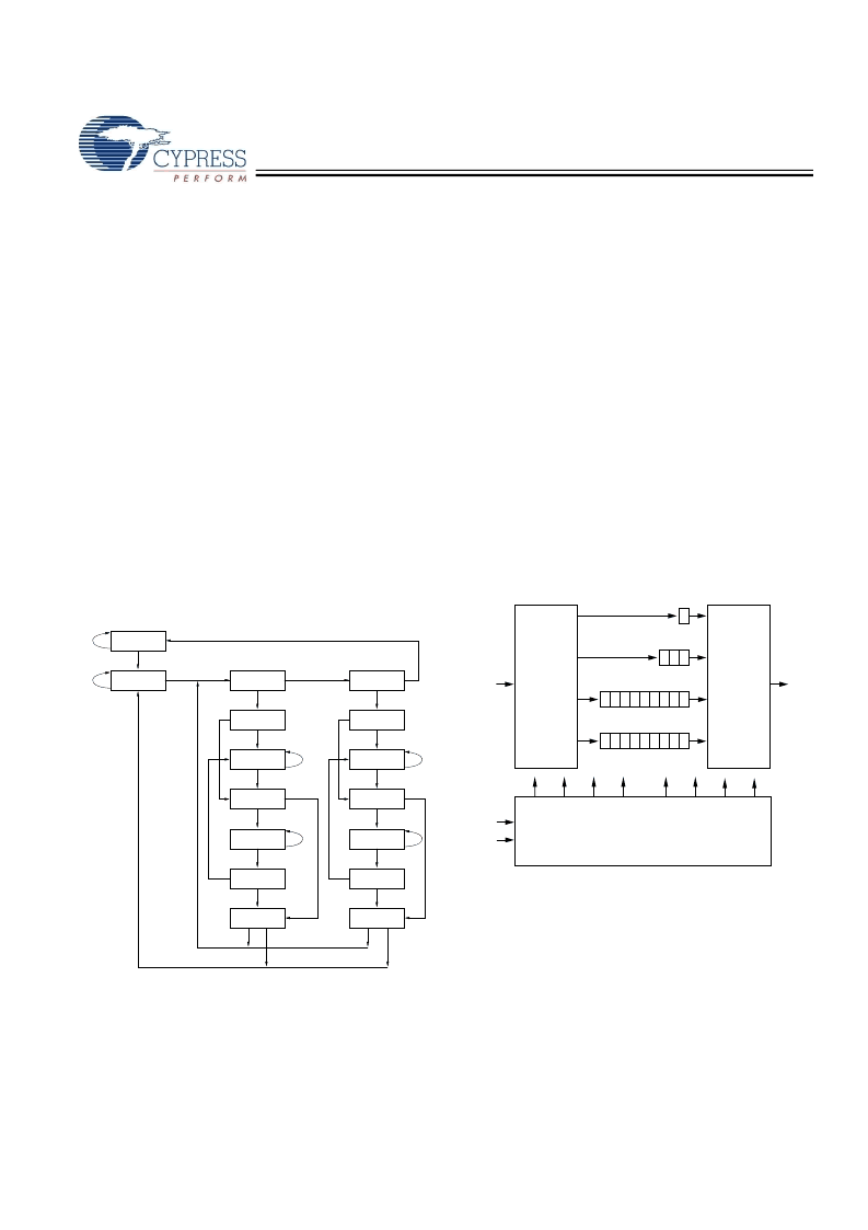
TAP Controller State Diagram
TEST-LOGIC
RESET
RUN-TEST/
IDLE
SELECT
DR-SCAN
SELECT
IR-SCAN
CAPTURE-DR
SHIFT-DR
CAPTURE-IR
SHIFT-IR
EXIT1-DR
PAUSE-DR
EXIT1-IR
PAUSE-IR
EXIT2-DR
UPDATE-DR
EXIT2-IR
UPDATE-IR
1
1
1
0
1
1
0
0
1
1
1
0
0
0
0
0
0
0
0
0
1
0
1
1
0
1
0
1
1
1
1
0
TAP Controller Block Diagram
Bypass Register
0
Instruction Register
0
1
2
Identification Register
0
1
2
29
30
31
.
.
.
Boundary Scan Register
0
1
2
.
.
x
.
.
.
Selection
Circuitry
TCK
TMS
TAP CONTROLLER
TDI
TDO
Selection
Circuitry
[+] Feedback
相关PDF资料 |
PDF描述 |
|---|---|
| CY7C1481V25-133BZC | 72-Mbit (2M x 36/4M x 18/1M x 72) Flow-Through SRAM |
| CY7C1481V25-133BZI | 72-Mbit (2M x 36/4M x 18/1M x 72) Flow-Through SRAM |
| CY7C1481V25-133BZXC | 72-Mbit (2M x 36/4M x 18/1M x 72) Flow-Through SRAM |
| CY7C1481V25-133BZXI | 72-Mbit (2M x 36/4M x 18/1M x 72) Flow-Through SRAM |
| CY7C1483V25 | 72-Mbit (2M x 36/4M x 18/1M x 72) Flow-Through SRAM |
相关代理商/技术参数 |
参数描述 |
|---|---|
| CY7C1481V33-100AXI | 制造商:Cypress Semiconductor 功能描述: |
| CY7C1482BV33-200BZI | 功能描述:静态随机存取存储器 72MB (4Mx18) 4.6v 200MHz 静态随机存取存储器 RoHS:否 制造商:Cypress Semiconductor 存储容量:16 Mbit 组织:1 M x 16 访问时间:55 ns 电源电压-最大:3.6 V 电源电压-最小:2.2 V 最大工作电流:22 uA 最大工作温度:+ 85 C 最小工作温度:- 40 C 安装风格:SMD/SMT 封装 / 箱体:TSOP-48 封装:Tray |
| CY7C1482BV33-250BZI | 制造商:Cypress Semiconductor 功能描述:2MX36, 3.3V SYNC PL SRAM - Bulk |
| CY7C148-35PC | 功能描述:1KX4 18-PIN POWER-DOWN SRAM RoHS:否 类别:集成电路 (IC) >> 存储器 系列:- 标准包装:1,000 系列:- 格式 - 存储器:EEPROMs - 串行 存储器类型:EEPROM 存储容量:4K (512 x 8) 速度:400kHz 接口:I²C,2 线串口 电源电压:2.7 V ~ 5.5 V 工作温度:-40°C ~ 85°C 封装/外壳:8-SOIC(0.173",4.40mm 宽) 供应商设备封装:8-MFP 包装:带卷 (TR) |
| CY7C148-45DC | 制造商:Cypress Semiconductor 功能描述:Static RAM, 1Kx4, 18 Pin, Ceramic, DIP |
发布紧急采购,3分钟左右您将得到回复。