- 您现在的位置:买卖IC网 > PDF目录223638 > CY7C343B-25JI (CYPRESS SEMICONDUCTOR CORP) OT PLD, 25 ns, PQCC44 PDF资料下载
参数资料
| 型号: | CY7C343B-25JI |
| 厂商: | CYPRESS SEMICONDUCTOR CORP |
| 元件分类: | PLD |
| 英文描述: | OT PLD, 25 ns, PQCC44 |
| 封装: | PLASTIC, LCC-44 |
| 文件页数: | 6/11页 |
| 文件大小: | 178K |
| 代理商: | CY7C343B-25JI |
CY7C343B
USE ULTRA37000TM FOR
ALL NEW DESIGNS
Document #: 38-03038 Rev. *B
Page 4 of 11
Programmable Interconnect Array
The Programmable Interconnect Array (PIA) solves inter-
connect limitations by routing only the signals needed by each
logic array block. The inputs to the PIA are the outputs of every
macrocell within the device and the I/O pin feedback of every
pin on the device.
Unlike masked or programmable gate arrays, which induce
variable delay dependent on routing, the PIA has a fixed delay.
This eliminates undesired skews among logic signals, which
may cause glitches in internal or external logic. The fixed
delay, regardless of programmable interconnect array config-
uration, simplifies design by ensuring that internal signal
skews or races are avoided. The result is simpler design imple-
mentation, often in a single pass, without the multiple internal
logic placement and routing iterations required for a program-
mable gate array to achieve design timing objectives.
Design Recommendations
Operation of the devices described herein with conditions
above those listed under “Absolute Maximum Ratings” may
cause permanent damage to the device. This is a stress rating
only and functional operation of the device at these or any
other conditions above those indicated in the operational
sections of this data sheet is not implied. Exposure to absolute
maximum ratings conditions for extended periods of time may
affect device reliability. The CY7C343B contains circuitry to
protect device pins from high static voltages or electric fields;
however, normal precautions should be taken to avoid
applying any voltage higher than maximum rated voltages.
For proper operation, input and output pins must be
constrained to the range GND < (VIN or VOUT) < VCC. Unused
inputs must always be tied to an appropriate logic level (either
VCC or GND). Each set of VCC and GND pins must be
connected together directly at the device. Power supply
decoupling capacitors of at least 0.2
F must be connected
between VCC and GND. For the most effective decoupling,
each VCC pin should be separately decoupled to GND, directly
at the device. Decoupling capacitors should have good
frequency response, such as monolithic ceramic types.
Timing Considerations
Unless otherwise stated, propagation delays do not include
expanders. When using expanders, add the maximum
expander delay tEXP to the overall delay. Similarly, there is an
additional tPIA delay for an input from an I/O pin when
compared to a signal from a straight input pin.
When calculating synchronous frequencies, use tS1 if all inputs
are on the input pins. When expander logic is used in the data
path, add the appropriate maximum expander delay, tEXP to
tS1. Determine which of 1/(tWH + tWL), 1/tCO1, or 1/(tEXP + tS1)
is the lowest frequency. The lowest of these frequencies is the
maximum data path frequency for the synchronous configu-
ration.
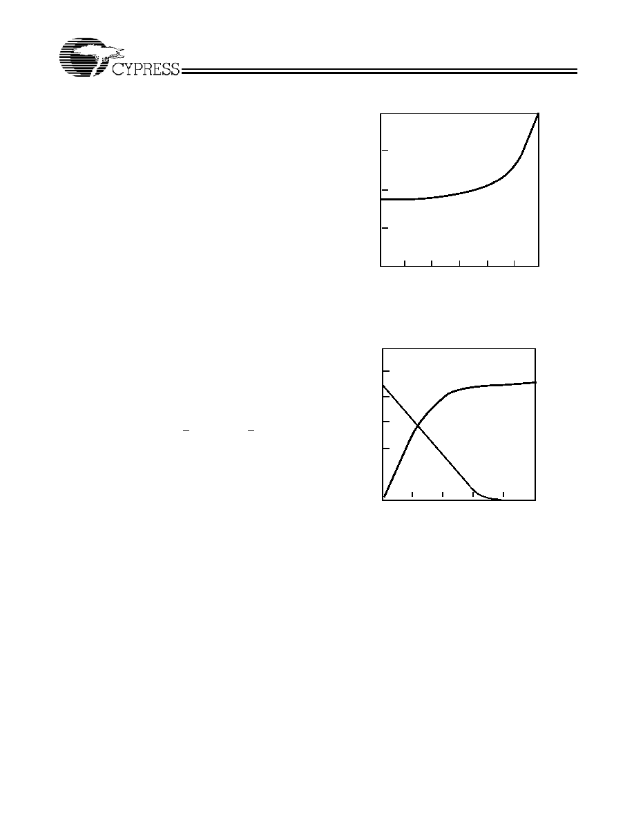
Typical ICC vs. fMAX
Output Drive Current
When calculating external asynchronous frequencies, use
tAS1 if all inputs are on dedicated input pins.
When expander logic is used in the data path, add the appro-
priate maximum expander delay, tEXP to tAS1. Determine
which of 1/(tAWH + tAWL), 1/tACO1, or 1/(tEXP + tAS1) is the
lowest frequency. The lowest of these frequencies is the
maximum data path frequency for the asynchronous configu-
ration.
The parameter tOH indicates the system compatibility of this
device when driving other synchronous logic with positive
input hold times, which is controlled by the same synchronous
clock. If tOH is greater than the minimum required input hold
time of the subsequent synchronous logic, then the devices
are guaranteed to function properly with a common
synchronous clock under worst-case environmental and
supply voltage conditions.
200
150
100
50
1 kHz
10 kHz
100 kHz
1 MHz
I CC
MAXIMUM FREQUENCY
10 MHz
0
50 MHz
100 Hz
ACTIVE
(mA)
Ty
p.
VCC = 5.0V
Room Temp.
01
2
3
4
I
OUT
P
UT
C
URRENT
(mA)
TYPICAL
VO OUTPUT VOLTAGE (V)
250
200
150
100
50
5
O
IOH
IOL
VCC = 5.0V
Room Temp.
相关PDF资料 |
PDF描述 |
|---|---|
| CY7C343B-30JC | OT PLD, 30 ns, PQCC44 |
| CY7C343B-30JI | OT PLD, 30 ns, PQCC44 |
| CY7C343B-35JC | OT PLD, 35 ns, PQCC44 |
| CY7C343B-35JI | OT PLD, 35 ns, PQCC44 |
| CY7C343B-25HC | UV PLD, 25 ns, CQCC44 |
相关代理商/技术参数 |
参数描述 |
|---|---|
| CY7C343B-30JC | 制造商:Cypress Semiconductor 功能描述:CPLD MAX? Family 1.25K Gates 64 Macro Cells 40MHz 0.65um Technology 5V 44-Pin PLCC |
| CY7C343B-35JI | 制造商:QP Semiconductor 功能描述: |
| CY7C344-15JC | 制造商:Cypress Semiconductor 功能描述: |
| CY7C344-15PC | 制造商:Cypress Semiconductor 功能描述:CPLD MAX? Family 600 Gates 32 Macro Cells 0.8um Technology 5V 28-Pin PDIP |
| CY7C344-20JC | 制造商:Cypress Semiconductor 功能描述:CPLD MAX? Family 600 Gates 32 Macro Cells 0.8um Technology 5V 28-Pin PLCC |
发布紧急采购,3分钟左右您将得到回复。