- 您现在的位置:买卖IC网 > PDF目录295396 > CY7C4205-10ACT (CYPRESS SEMICONDUCTOR CORP) 256 X 18 OTHER FIFO, 8 ns, PQFP64 PDF资料下载
参数资料
| 型号: | CY7C4205-10ACT |
| 厂商: | CYPRESS SEMICONDUCTOR CORP |
| 元件分类: | FIFO |
| 英文描述: | 256 X 18 OTHER FIFO, 8 ns, PQFP64 |
| 封装: | 14 X 14 MM, PLASTIC, TQFP-64 |
| 文件页数: | 19/25页 |
| 文件大小: | 412K |
| 代理商: | CY7C4205-10ACT |
CY7C4425/4205/4215
CY7C4225/4235/4245
3
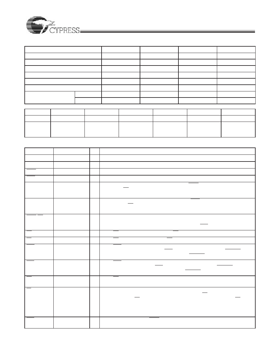
Selection Guide
7C42X5-10
7C42X5-15
7C42X5-25
7C42X5-35
Maximum Frequency (MHz)
100
66.7
40
28.6
Maximum Access Time (ns)
8
10
15
20
Minimum Cycle Time (ns)
10
15
25
35
Minimum Data or Enable Set-Up (ns)
3
4
6
7
Minimum Data or Enable Hold (ns)
0.5
1
2
Maximum Flag Delay (ns)
8
10
15
20
Operating Current (ICC2)
(mA) @ freq=20MHz
Commercial
45
Industrial
50
CY7C4425
CY7C4205
CY7C4215
CY7C4225
CY7C4235
CY7C4245
Density
64 x 18
256 x 18
512 x 18
1K x 18
2K x 18
4K x 18
Packages
68-pin PLCC
64-pin TQFP
(10x10/14x14)
68-pin PLCC
64-pin TQFP
(10x10/14x14)
68-pin PLCC
64-pin TQFP
(10x10/14x14)
68-pin PLCC
64-pin TQFP
(10x10/14x14)
68-pin PLCC
64-pin TQFP
(10x10/14x14)
68-pin PLCC
64-pin TQFP
(10x10/14x14)
Pin Definitions
Signal Name
Description
I/O
Function
D0–17
Data Inputs
I
Data inputs for an 18-bit bus
Q0–17
Data Outputs
O
Data outputs for an 18-bit bus
WEN
Write Enable
I
Enables the WCLK input
REN
Read Enable
I
Enables the RCLK input
WCLK
Write Clock
I
The rising edge clocks data into the FIFO when WEN is LOW and the FIFO is not
Full. When LD is asserted, WCLK writes data into the programmable flag-offset
register.
RCLK
Read Clock
I
The rising edge clocks data out of the FIFO when REN is LOW and the FIFO is not
Empty. When LD is asserted, RCLK reads data out of the programmable flag-off-
set register.
WXO/HF
Write Expansion
Out/Half Full Flag
O
Dual-Mode Pin:
Single device or width expansion - Half Full status flag.
Cascaded - Write Expansion Out signal, connected to WXI of next device.
EF
Empty Flag
O
When EF is LOW, the FIFO is empty. EF is synchronized to RCLK.
FF
Full Flag
O
When FF is LOW, the FIFO is full. FF is synchronized to WCLK.
PAE
Programmable
Almost Empty
O
When PAE is LOW, the FIFO is almost empty based on the almost-empty offset
value programmed into the FIFO. PAE is asynchronous when VCC/SMODE is tied
to VCC; it is synchronized to RCLK when VCC/SMODE is tied to VSS.
PAF
Programmable
Almost Full
O
When PAF is LOW, the FIFO is almost full based on the almost full offset value
programmed into the FIFO. PAF is asynchronous when VCC/SMODE is tied to
VCC; it is synchronized to WCLK when VCC/SMODE is tied to VSS.
LD
Load
I
When LD is LOW, D0 - 17 (O0 - 17) are written (read) into (from) the programma-
ble-flag-offset register.
FL/RT
First Load/
Retransmit
I
Dual-Mode Pin:
Cascaded - The first device in the daisy chain will have FL tied to VSS; all other
devices will have FL tied to VCC. In standard mode of width expansion, FL is tied
to VSS on all devices.
Not Cascaded - Tied to VSS. Retransmit function is also available in standalone
mode by strobing RT.
WXI
Write Expansion
Input
I
Cascaded - Connected to WXO of previous device.
Not Cascaded - Tied to VSS.
相关PDF资料 |
PDF描述 |
|---|---|
| CY7C4235V-25JC | 2K X 18 OTHER FIFO, 15 ns, PQCC68 |
| CY7C4241-35JC | 4K X 9 OTHER FIFO, 20 ns, PQCC32 |
| CY7C4421-15JIT | 64 X 9 OTHER FIFO, 10 ns, PQCC32 |
| CY7C4421-25AC | 64 X 9 OTHER FIFO, 15 ns, PQFP32 |
| CY7C510-65LMB | Multiplier/Accumulator |
相关代理商/技术参数 |
参数描述 |
|---|---|
| CY7C4205-10AXC | 功能描述:先进先出 256x18 IDT Compat SYNC 先进先出 COM RoHS:否 制造商:IDT 电路数量: 数据总线宽度:18 bit 总线定向:Unidirectional 存储容量:4 Mbit 定时类型:Synchronous 组织:256 K x 18 最大时钟频率:100 MHz 访问时间:10 ns 电源电压-最大:3.6 V 电源电压-最小:6 V 最大工作电流:35 mA 最大工作温度:+ 85 C 封装 / 箱体:TQFP-80 封装: |
| CY7C4205-10AXCT | 功能描述:先进先出 256x18 IDT Compat SYNC 先进先出 COM RoHS:否 制造商:IDT 电路数量: 数据总线宽度:18 bit 总线定向:Unidirectional 存储容量:4 Mbit 定时类型:Synchronous 组织:256 K x 18 最大时钟频率:100 MHz 访问时间:10 ns 电源电压-最大:3.6 V 电源电压-最小:6 V 最大工作电流:35 mA 最大工作温度:+ 85 C 封装 / 箱体:TQFP-80 封装: |
| CY7C4205-15AC | 制造商:Cypress Semiconductor 功能描述: |
| CY7C4205-15ACT | 制造商:Cypress Semiconductor 功能描述: |
| CY7C4205-15ASC | 制造商:Cypress Semiconductor 功能描述:FIFO Mem Sync Dual Depth/Width Uni-Dir 256 x 18 64-Pin TQFP 制造商:Rochester Electronics LLC 功能描述:256 X 18 68 PIN IDT COMPAT SYNC FIFO - Bulk |
发布紧急采购,3分钟左右您将得到回复。