- 您现在的位置:买卖IC网 > PDF目录223639 > CYW2332BCI (CYPRESS SEMICONDUCTOR CORP) PLL FREQUENCY SYNTHESIZER, 1200 MHz, QCC24 PDF资料下载
参数资料
| 型号: | CYW2332BCI |
| 厂商: | CYPRESS SEMICONDUCTOR CORP |
| 元件分类: | PLL合成/DDS/VCOs |
| 英文描述: | PLL FREQUENCY SYNTHESIZER, 1200 MHz, QCC24 |
| 封装: | 3.50 X 4.50 MM, CSP-24 |
| 文件页数: | 11/13页 |
| 文件大小: | 228K |
| 代理商: | CYW2332BCI |
CYW2332
PRELIMINARY
Document #: 38-07238 Rev. **
Page 7 of 13
Notes:
6.
The MSB is loaded in first.
7.
Low count ratios may violate frequency limits of the phase detector.
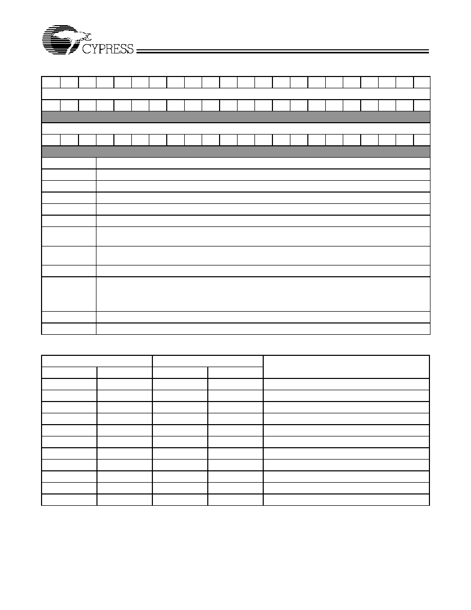
Table 2. Shift Register Configuration[6]
1
2
3
456789
10
11
12
13
14
15
16
17
18
19
20
21
22
Reference Counter and Configuration Bits
CNT1 CNT2
R1
R2
R3
R4
R5
R6
R7
R8
R9
R10 R11 R12 R13 R14 R15
FC
IDO
TS
LD
FO
Programmable Counter Bits
CNT1 CNT2
A1
A2
A3
A4
A5
A6
A7
B1
B2
B3
B4
B5
B6
B7
B8
B9
B10 B11 PRE PD
Bit(s) Name
Function
CNT1, CNT2
Control Bits: Directs programming data to PLL1 (high frequency) or PLL2 (low frequency).
R1–R15
Reference Counter Setting Bits: 15 bits, R = 3 to 32767.[7]
FC
Phase Sense of the Phase Detector: Set to match the VCO polarity, H = + (Positive VCO transfer function).
IDO
Charge Pump Setting Bit: IDO HIGH = 3.8 mA, IDO LOW = 1 mA at VP = 3V.
TS
Hi-Impedance State Bit: Makes DO Hi-Impedance for PLL1 and PLL2 when HIGH.
LD
Lock Detect: Directs the lock detect signal source pin 10. Pin 10 is HIGH with narrow low excursions when
locked. When not locked, this pin is LOW.
FO
Frequency Out: This bit can be set to read out reference or programmable divider at the LD pin for test
purposes.
PRE
Prescaler Divide Bit: For PLL1: LOW = 64/65 and HIGH = 128/129. For PLL2: LOW = 8/9 and HIGH = 16/17.
PD
Power-down: LOW = power-up and HIGH = power-down. FIN is at a high-impedance state, respective B
counter is disabled, forces DO outputs to Hi-Impedance and phase comparators are disabled. The reference
counter is disabled and the OSC input is high-impedance after both PLLs are powered down. Data can be
input and latched in the power-down state.
A1–A7
Swallow Counter Divide Ratio: A = 0 to 127 for PLL1 and 0 to 15 for PLL2.
B1–B11
Programmable Counter Divide Ratio: B = 3 to 2047.[7]
Table 3. FO/LD Pin Truth Table
FO (Bit 22)
LD (Bit 21)
FO/LD Pin Output State
PLL1
PLL2
PLL1
PLL2
0000
Disable
0001
PLL2 Lock Detect
0010
PLL1 Lock Detect
0011
PLL1/PLL2 Lock Detect
0
1
X
0
PLL2 Reference Divider Output
1
0
X
0
PLL1 Reference Divider Output
0
1
X
1
PLL2 Programmable Divider Output
1
0
X
1
PLL1 Programmable Divider Output
1101
Test PLL2 Counter Reset
1110
Test PLL1 Counter Reset
1111
Test PLL1/PLL2 Counter Reset
相关PDF资料 |
PDF描述 |
|---|---|
| CYW255OXC | 255 SERIES, LOW SKEW CLOCK DRIVER, 24 TRUE OUTPUT(S), 0 INVERTED OUTPUT(S), PDSO48 |
| CYW256OXCT | 256 SERIES, LOW SKEW CLOCK DRIVER, 12 TRUE OUTPUT(S), 0 INVERTED OUTPUT(S), PDSO28 |
| D01-9970121 | SIP1, IC SOCKET |
| D01-9974842 | SIP48, IC SOCKET |
| D03-28-T-A-A-2 | IC SOCKET |
相关代理商/技术参数 |
参数描述 |
|---|---|
| CYW2338 | 制造商:CYPRESS 制造商全称:Cypress Semiconductor 功能描述:Dual Serial Input PLL with 2.5- and 1.1-GHz Prescalers |
| CYW2338ZI | 制造商:Cypress Semiconductor 功能描述: |
| CYW2338ZIT | 制造商:Cypress Semiconductor 功能描述: |
| CYW255OXC | 功能描述:时钟缓冲器 200MhZ-24 Out Buff 4 DDR3 SDRAM DIMMS RoHS:否 制造商:Texas Instruments 输出端数量:5 最大输入频率:40 MHz 传播延迟(最大值): 电源电压-最大:3.45 V 电源电压-最小:2.375 V 最大功率耗散: 最大工作温度:+ 85 C 最小工作温度:- 40 C 封装 / 箱体:LLP-24 封装:Reel |
| CYW255OXCT | 功能描述:时钟缓冲器 200MhZ-24 Out Buff 4 DDR3 SDRAM DIMMS RoHS:否 制造商:Texas Instruments 输出端数量:5 最大输入频率:40 MHz 传播延迟(最大值): 电源电压-最大:3.45 V 电源电压-最小:2.375 V 最大功率耗散: 最大工作温度:+ 85 C 最小工作温度:- 40 C 封装 / 箱体:LLP-24 封装:Reel |
发布紧急采购,3分钟左右您将得到回复。