参数资料
| 型号: | D2-24044-MR |
| 厂商: | Intersil |
| 文件页数: | 2/20页 |
| 文件大小: | 0K |
| 描述: | IC DGTL AMP AUDIO PWR D 38HTSSOP |
| 标准包装: | 50 |
| 系列: | D2Audio™ |
| 类型: | D 类 |
| 输出类型: | 2-通道(立体声)或 4 通道(四路) |
| 在某负载时最大输出功率 x 通道数量: | 30W x 2 @ 8 欧姆 |
| 电源电压: | 9 V ~ 26 V |
| 安装类型: | 表面贴装 |
| 供应商设备封装: | 38-HTSSOP |
| 封装/外壳: | 38-TFSOP (0.173",4.40mm 宽)裸露焊盘 |
| 包装: | 管件 |
10
FN7678.0
September 3, 2010
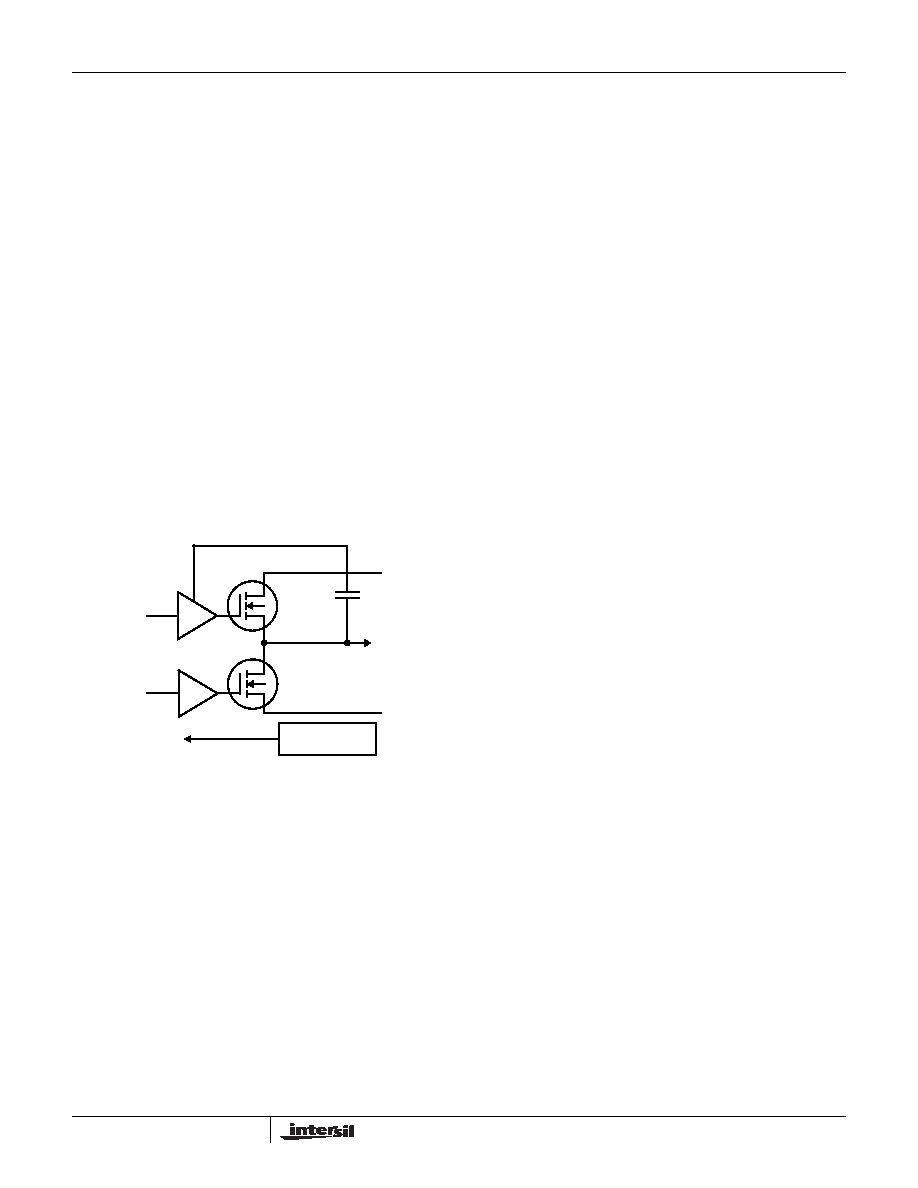
Functional Overview
The devices include four independent output stages
(Figure 9) that are each implemented using a high side
(to positive VDDHV supply) and a low side (to HV supply
ground) FET pair. Drivers and overcurrent monitoring are
included in each of these four output stages. Depending
on the selected configuration mode, these four stages
can be used independently as single half-bridge outputs,
or as pairs for full-bridge outputs.
Digital PWM inputs are connected to the PWM input pins,
where their signals are routed through the configuration
select logic to the individual output FETs and drivers.
On-chip temperature and undervoltage monitoring, and
individual per-output current monitoring provides
protection and status reporting outputs to the system
controller.
Upon application of power, the on-chip voltage sensors
monitor presence of the required power voltages. Until all
voltages are at their design specifications, the outputs
remain off and floating.
After supply voltages are within limits and stable, the
output configuration is set by the logic levels at the
OCFG0 and OCFG1 input pins, and the PWM inputs are
routed to their appropriate output stage FETs.
Output Options
The D2-24044 devices provide four configuration options
for the outputs. These options are selected by strapping
the OCFG0 and OCFG1 pins high or low. These defined
configurations include:
2 Channels of Full Bridge, 4-Quadrant Outputs,
2 Channels of Full Bridge, 2-Quadrant Outputs
4 Channels of Half-Bridge Outputs
2 Channels Half-Bridge, Plus 1 Channel Full Bridge
When a configuration is set that includes a full-bridge
output, each input channel’s PWM input signal is routed
to the high and low side FETs, appropriate for that full
bridge operation. Note however, that the device can be
configured as 4 independent half-bridge outputs (using
mode “11” as described in the configuration assignment
table on page 14) and two of those outputs can be used
in a full bridge configuration, simply by connecting the
appropriate PWM input pins to the input source. This
allows flexibility in applications where combinations may
be desired other than the four defined by the output
configuration modes.
Power Supply Requirements
The device operates from two supply voltages:
PWMVDD is a nominal 3.3V supply voltage, and
operates the logic and control.
HVDD (HVDD[A:D], and VDDHV) is the “high
voltage” used for operating the output power stages.
Individual HVDD and its ground (HGND) pins are
included for each of the four power stage outputs,
providing channel isolation and low impedance source
connections to each of the outputs. A separate VDDHV
pin is used for the output drivers, and is the source for
the on-chip regulated 5V source needed for the drivers.
All the HVDD/VDDHV pins connect to the same voltage
source.
PWMVDD is the reference for the PWM inputs and device
control logic, and is the same voltage as used by the
PWM/system controller.
High Side Gate Drive Voltage
An on-chip bootstrap circuit provides the high-side gate
drive voltage used by each output stage. A pin is
included for each output channel (HSBS[A:D]) for
connection of a capacitor (nominal, 0.22μF/50V) from
this pin to that channel’s PWM output. The charge
pumping actions uses this capacitor to filter and hold this
gate drive voltage, and enables amplifier operation
without need of connection to an additional power supply
voltage.
Supply Bypass Connection
Power supply bypass capacitors should be connected
across each of the power supply connection pins, as:
Four HVDD power pins and their respective HGND
ground pins. These should be a parallel combination
of a nominal 100μF and 0.1μF capacitors, located as
close as possible to the HVDD/HGND pin pair.
A 0.1μF capacitor also is to connect at the VDDHV
pin.
The PWMVDD power pin should include a 1μF and
0.1μF capacitor.
REG5V
The on-chip gate drive power supply operates from the
VDDHV power input, to produce the 5V supply voltage.
The REG5V pin is used for external capacitor connection
to filter this regulated voltage. A 1.0μF and 0.1μF
capacitor should be connected to this pin, and the
connection should be made as close as practical to the
pin. No other connection is to be made to this pin.
FIGURE 9. OUTPUT STAGE
HSBSA
HIGH-SIDE
PWM DRIVE
LOW SIDE
PWM DRIVE
nERROR
OVERCURRENT
HGND
(GND)
LOW
SIDE
FET
HIGH
SIDE
FET
(+)
HVDD
OUT
D2-24044
相关PDF资料 |
PDF描述 |
|---|---|
| D2-45157-QR | IC DGTL AMP PWM CTRLR 68QFN |
| DS1080CLU+ | IC CRYSTAL MULTIPLIER SS 8-MSOP |
| DS1080LU+A00 | IC CRYSTAL MULT SS 8-USOP |
| DS1085LZ-12+ | IC ECONOSCILLATOR SYNTH 8-SOIC |
| DS1085Z-25+ | IC ECONOSCILLATOR SYNTH 8-SOIC |
相关代理商/技术参数 |
参数描述 |
|---|---|
| D2-24044-MR-T | 功能描述:音频放大器 LW-PWR CLASS-AMPLIFI 3 8LD HTSSOP 4 4X9 7 RoHS:否 制造商:STMicroelectronics 产品:General Purpose Audio Amplifiers 输出类型:Digital 输出功率: THD + 噪声: 工作电源电压:3.3 V 电源电流: 最大功率耗散: 最大工作温度: 安装风格:SMD/SMT 封装 / 箱体:TQFP-64 封装:Reel |
| D224E | 制造商:MPD 制造商全称:MicroPower Direct, LLC 功能描述:Low Cost, 2W SIP Single & Dual Output DC/DC Converters |
| D224ED | 制造商:MPD 制造商全称:MicroPower Direct, LLC 功能描述:Very Low Cost, 2W SIP Dual Isolated Output DC/DC Converters |
| D224EI | 制造商:MPD 制造商全称:MicroPower Direct, LLC 功能描述:Low Cost, 2W SIP High Isolation DC/DC Converters |
| D224ERW | 制造商:MPD 制造商全称:MicroPower Direct, LLC 功能描述:Low Cost, Miniature 2W SIP, Wide Input DC/DC Con vert ers |
发布紧急采购,3分钟左右您将得到回复。