- 您现在的位置:买卖IC网 > PDF目录170654 > DAC5311IDCKTG4 (TEXAS INSTRUMENTS INC) SERIAL INPUT LOADING, 12 us SETTLING TIME, 8-BIT DAC, PDSO6 PDF资料下载
参数资料
| 型号: | DAC5311IDCKTG4 |
| 厂商: | TEXAS INSTRUMENTS INC |
| 元件分类: | DAC |
| 英文描述: | SERIAL INPUT LOADING, 12 us SETTLING TIME, 8-BIT DAC, PDSO6 |
| 封装: | GREEN, PLASTIC, SC-70, 6 PIN |
| 文件页数: | 21/42页 |
| 文件大小: | 2283K |
| 代理商: | DAC5311IDCKTG4 |
第1页第2页第3页第4页第5页第6页第7页第8页第9页第10页第11页第12页第13页第14页第15页第16页第17页第18页第19页第20页当前第21页第22页第23页第24页第25页第26页第27页第28页第29页第30页第31页第32页第33页第34页第35页第36页第37页第38页第39页第40页第41页第42页
SERIAL INTERFACE
DACx311 Input Shift Register
DACx311 SYNC Interrupt
InvalidWriteSequence:
HIGHbefore16thFallingEdge
SYNC
ValidWriteSequence:
OutputUpdateson16thFallingEdge
CLK
SYNC
D
IN
DB15
DB0
DB15
DB0
SBAS442 – AUGUST 2008 ................................................................................................................................................................................................ www.ti.com
the DACx311 compatible with high-speed DSPs. On
the 16th falling edge of the serial clock, the last data
The DACx311 has a 3-wire serial interface (SYNC,
bit is clocked in and the programmed function is
SCLK, and DIN) compatible with SPI, QSPI, and
executed.
Microwire interface standards, as well as most DSPs.
See the Serial Write Operation timing diagram for an
At this point, the SYNC line may be kept low or
example of a typical write sequence.
brought high. In either case, it must be brought high
for a minimum of 20ns before the next write
sequence so that a falling edge of SYNC can initiate
the next write sequence. As previously mentioned, it
The input shift register is 16 bits wide, as shown in
must be brought high again before the next write
Table 2. The first two bits (PD0 and PD1) are
sequence.
reserved control bits that set the desired mode of
operation
(normal
mode
or
any
one
of
three
power-down modes) as indicated in Table 5.
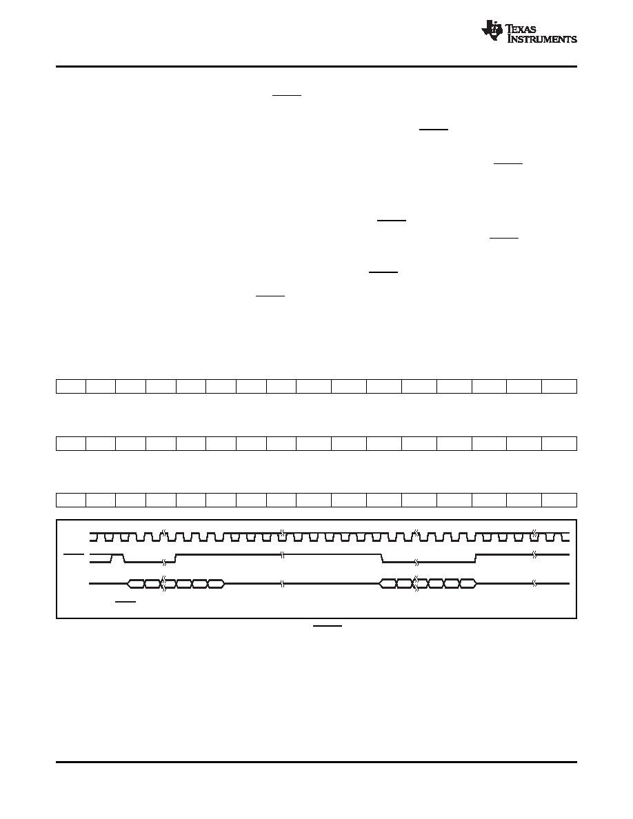
In a normal write sequence, the SYNC line is kept
The remaining data bits are either 12 (DAC7311), 10
low for at least 16 falling edges of SCLK and the DAC
(DAC6311), or 8 (DAC5311) data bits, followed by
is updated on the 16th falling edge. However,
don't care bits, as shown in Table 2, Table 3, and
bringing SYNC high before the 16th falling edge acts
Table 4, respectively.
as an interrupt to the write sequence. The shift
register is reset and the write sequence is seen as
The write sequence begins by bringing the SYNC line
invalid. Neither an update of the DAC register
low. Data from the DIN line are clocked into the 16-bit
contents nor a change in the operating mode occurs,
shift register on each falling edge of SCLK. The serial
as shown in Figure 112.
clock frequency can be as high as 50MHz, making
Table 2. DAC5311 8-Bit Data Input Register
DB15
DB14
DB6
DB5
DB0
PD1
PD0
D7
D6
D5
D4
D3
D2
D1
D0
X
Table 3. DAC6311 10-Bit Data Input Register
DB15
DB14
DB4
DB3
DB0
PD1
PD0
D9
D8
D7
D6
D5
D4
D3
D2
D1
D0
X
Table 4. DAC7311 12-Bit Data Input Register
DB15
DB14
DB2
DB1
DB0
PD1
PD0
D11
D10
D9
D8
D7
D6
D5
D4
D3
D2
D1
D0
X
Figure 112. DACx311 SYNC Interrupt Facility
28
Copyright 2008, Texas Instruments Incorporated
Product Folder Link(s): DAC5311 DAC6311 DAC7311
相关PDF资料 |
PDF描述 |
|---|---|
| DAC5652AIPFBRG4 | DUAL, PARALLEL, WORD INPUT LOADING, 0.02 us SETTLING TIME, 10-BIT DAC, PQFP48 |
| DAC5672AIPFBRG4 | DUAL, PARALLEL, WORD INPUT LOADING, 0.02 us SETTLING TIME, 14-BIT DAC, PQFP48 |
| DAC5672AIPFBR | DUAL, PARALLEL, WORD INPUT LOADING, 0.02 us SETTLING TIME, 14-BIT DAC, PQFP48 |
| DAC5687IPZP | PARALLEL, WORD INPUT LOADING, 0.0104 us SETTLING TIME, 16-BIT DAC, PQFP100 |
| DAC5687IPZPG4 | PARALLEL, WORD INPUT LOADING, 0.0104 us SETTLING TIME, 16-BIT DAC, PQFP100 |
相关代理商/技术参数 |
参数描述 |
|---|---|
| DAC5311-Q1 | 制造商:TI 制造商全称:Texas Instruments 功能描述:1.8 V to 5.5 V, 80 mA, 8 BIT, LOW POWER, SINGLE CHANNEL, DIGITAL-TO-ANALOG CONVERTER |
| DAC540H68Y WAF | 制造商:ON Semiconductor 功能描述: |
| DAC5571 | 制造商:TI 制造商全称:Texas Instruments 功能描述:+2.7 V to +5.5 V, I2C INTERFACE, VOLTAGE OUTPUT, 8-BIT DIGITAL-TO-ANALOG CONVERTER |
| DAC5571_07 | 制造商:TI 制造商全称:Texas Instruments 功能描述:+2.7 V to +5.5 V, I2C INTERFACE, VOLTAGE OUTPUT, 8-BIT DIGITAL-TO-ANALOG CONVERTER |
| DAC5571EVM | 功能描述:数据转换 IC 开发工具 DAC5571 Eval Mod RoHS:否 制造商:Texas Instruments 产品:Demonstration Kits 类型:ADC 工具用于评估:ADS130E08 接口类型:SPI 工作电源电压:- 6 V to + 6 V |
发布紧急采购,3分钟左右您将得到回复。