- 您现在的位置:买卖IC网 > PDF目录295418 > DAC716UB/1K SERIAL INPUT LOADING, 6 us SETTLING TIME, 16-BIT DAC, PDSO16 PDF资料下载
参数资料
| 型号: | DAC716UB/1K |
| 元件分类: | DAC |
| 英文描述: | SERIAL INPUT LOADING, 6 us SETTLING TIME, 16-BIT DAC, PDSO16 |
| 封装: | GREEN, PLASTIC, SOIC-16 |
| 文件页数: | 15/16页 |
| 文件大小: | 181K |
| 代理商: | DAC716UB/1K |
8
DAC716
DAC716 CALIBRATION VALUES
1 LEAST SIGNIFICANT BIT = 152
V
DIGITAL INPUT CODE
ANALOG OUTPUT (V)
STRAIGHT BINARY
UNIPOLAR 10V RANGE
DESCRIPTION
FFFFH
+9.999695
+ Full Scale –1LSB
|
8000
H
+5.000000
Half Scale
0000H
0.000000
Unipolar Zero
TABLE I. Digital Input and Analog Output Voltage Calibra-
tion Values.
INSTALLATION
GENERAL CONSIDERATIONS
Due to the high precision of these D/A converters, system
design problems such as grounding and contact resistance
become very important. A 16-bit converter with a 10V full-
scale range has a 1LSB value of 152
V. With a load current
of 5mA, series wiring and connector resistance of only
60m
will cause a voltage drop of 300V. To understand
what this means in terms of a system layout, the resistivity
of a typical 1 ounce copper-clad printed circuit board is 1/2
m
per square. For a 5mA load, a 0.1 inch wide printed
circuit conductor 0.6 inches long will result in a voltage drop
of 150
V.
The analog output of DAC716 has an LSB size of 152
V
(–96dB). The rms noise floor of the D/A should remain below
this level in the frequency range of interest. The DAC716’s
output noise spectral density (which includes the noise contrib-
uted by the internal reference) is shown in the Typical Perfor-
mance Curves section.
Wiring to high-resolution D/A converters should be routed
to provide optimum isolation from sources of RFI and EMI.
The key to elimination of RF radiation or pickup is small
loop area. Signal leads and their return conductors should be
kept close together such that they present a small capture
cross-section for any external field. Wire-wrap construction
is not recommended.
POWER SUPPLY AND
REFERENCE CONNECTIONS
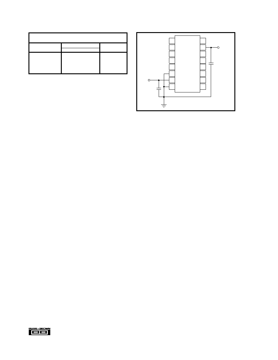
Power supply decoupling capacitors should be added as
shown in Figure 4. Best performance occurs using a 1 to
10
F tantalum capacitor at –V
CC. Applications with less
critical settling time may be able to use 0.01
F at –V
CC
as well as at +VCC. The capacitors should be located
close to the package.
The DAC716 has separate ANALOG COMMON and DIGI-
TAL COMMON pins. The current through DCOM is mostly
switching transients and are up to 1mA peak in amplitude.
The current through ACOM is typically 5
A for all codes.
Use separate analog and digital ground planes with a single
interconnection point to minimize ground loops. The analog
FIGURE 4. Power Supply Connections.
1
2
3
4
5
6
7
8
16
15
14
13
12
11
10
9
1F
DAC716
DCOM
+V
CC
ACOM
–V
CC
+12V to +15V
–12V to –15V
+
pins are located adjacent to each other to help isolate analog
from digital signals. Analog signals should be routed as far
as possible from digital signals and should cross them at
right angles. A solid analog ground plane around the D/A
package, as well as under it in the vicinity of the analog and
power supply pins, will isolate the D/A from switching
currents. It is recommended that DCOM and ACOM be
connected directly to the ground planes under the package.
If several DAC716s are used or if the DAC716 shares
supplies with other components, connecting the ACOM and
DCOM lines together at the power supplies only rather than
at each chip, may give better results.
LOAD CONNECTIONS
Since the reference point for VOUT and VREF OUT is the
ACOM pin, it is important to connect the D/A converter load
directly to the ACOM pin. Refer to Figure 5.
Lead and contact resistances are represented by R1 through
R3. As long as the load resistance RL is constant, R1 simply
introduces a gain error and can be removed by gain adjust-
ment of the D/A or system-wide gain calibration. R2 is part
of RL if the output voltage is sensed at ACOM.
In some applications it is impractical to return the load to the
ACOM pin of the D/A converter. Sensing the output voltage
at the SYSTEM GROUND point is reasonable, because there
is no change in DAC716 ACOM current, provided that R3 is
a low-resistance ground plane or conductor. In this case you
may wish to connect DCOM to SYSTEM GROUND as well.
GAIN AND OFFSET ADJUST
Connections Using Potentiometers
GAIN and OFFSET adjust pins provide for trim using
external potentiometers. 15-turn potentiometers provide suf-
ficient resolution. Range of adjustment of these trims is at
least
±0.3% of Full Scale Range. Refer to Figure 6.
相关PDF资料 |
PDF描述 |
|---|---|
| DAC716UL | SERIAL INPUT LOADING, 6 us SETTLING TIME, 16-BIT DAC, PDSO16 |
| DAC7512E/250 | SERIAL INPUT LOADING, 12 us SETTLING TIME, 12-BIT DAC, PDSO8 |
| DAC7512N/250 | SERIAL INPUT LOADING, 12 us SETTLING TIME, 12-BIT DAC, PDSO6 |
| DAC7512N/3K | SERIAL INPUT LOADING, 12 us SETTLING TIME, 12-BIT DAC, PDSO6 |
| DAC7512E/250 | SERIAL INPUT LOADING, 8 us SETTLING TIME, 12-BIT DAC, PDSO8 |
相关代理商/技术参数 |
参数描述 |
|---|---|
| DAC716UBG4 | 功能描述:数模转换器- DAC 16-Bit w/Ser Data Interface RoHS:否 制造商:Texas Instruments 转换器数量:1 DAC 输出端数量:1 转换速率:2 MSPs 分辨率:16 bit 接口类型:QSPI, SPI, Serial (3-Wire, Microwire) 稳定时间:1 us 最大工作温度:+ 85 C 安装风格:SMD/SMT 封装 / 箱体:SOIC-14 封装:Tube |
| DAC716UG4 | 功能描述:数模转换器- DAC 16-Bit w/Ser Data Interface RoHS:否 制造商:Texas Instruments 转换器数量:1 DAC 输出端数量:1 转换速率:2 MSPs 分辨率:16 bit 接口类型:QSPI, SPI, Serial (3-Wire, Microwire) 稳定时间:1 us 最大工作温度:+ 85 C 安装风格:SMD/SMT 封装 / 箱体:SOIC-14 封装:Tube |
| DAC716UK | 功能描述:数模转换器- DAC 16-Bit w/Ser Data Interface RoHS:否 制造商:Texas Instruments 转换器数量:1 DAC 输出端数量:1 转换速率:2 MSPs 分辨率:16 bit 接口类型:QSPI, SPI, Serial (3-Wire, Microwire) 稳定时间:1 us 最大工作温度:+ 85 C 安装风格:SMD/SMT 封装 / 箱体:SOIC-14 封装:Tube |
| DAC716UK/1K | 功能描述:数模转换器- DAC 16-Bit w/Ser Data Interface RoHS:否 制造商:Texas Instruments 转换器数量:1 DAC 输出端数量:1 转换速率:2 MSPs 分辨率:16 bit 接口类型:QSPI, SPI, Serial (3-Wire, Microwire) 稳定时间:1 us 最大工作温度:+ 85 C 安装风格:SMD/SMT 封装 / 箱体:SOIC-14 封装:Tube |
| DAC716UK/1KG4 | 功能描述:数模转换器- DAC 16-Bit w/Ser Data Interface RoHS:否 制造商:Texas Instruments 转换器数量:1 DAC 输出端数量:1 转换速率:2 MSPs 分辨率:16 bit 接口类型:QSPI, SPI, Serial (3-Wire, Microwire) 稳定时间:1 us 最大工作温度:+ 85 C 安装风格:SMD/SMT 封装 / 箱体:SOIC-14 封装:Tube |
发布紧急采购,3分钟左右您将得到回复。