- 您现在的位置:买卖IC网 > PDF目录170654 > DAC7654YTG4 (TEXAS INSTRUMENTS INC) SERIAL INPUT LOADING, 12 us SETTLING TIME, 16-BIT DAC, PQFP64 PDF资料下载
参数资料
| 型号: | DAC7654YTG4 |
| 厂商: | TEXAS INSTRUMENTS INC |
| 元件分类: | DAC |
| 英文描述: | SERIAL INPUT LOADING, 12 us SETTLING TIME, 16-BIT DAC, PQFP64 |
| 封装: | GREEN, PLASTIC, LQFP-64 |
| 文件页数: | 16/33页 |
| 文件大小: | 804K |
| 代理商: | DAC7654YTG4 |
第1页第2页第3页第4页第5页第6页第7页第8页第9页第10页第11页第12页第13页第14页第15页当前第16页第17页第18页第19页第20页第21页第22页第23页第24页第25页第26页第27页第28页第29页第30页第31页第32页第33页
DAC7654
SBAS263A NOVEMBER 2003 REVISED DECEMBER 2005
www.ti.com
23
The DAC code, quick load control, and address are provided
via a 24-bit serial interface (see Table 3; also see Figure 58,
page 25). The first two bits select the input register that will
be updated when LOAD goes low. The third bit is a Quick
Load bit; if high, the code in the shift register is loaded into
all of the DAC input registers when the LOAD signal goes
low. If the Quick Load bit is low, the content of shift register
is loaded only to the DAC input register that is addressed.
The Quick Load bit is followed by five unused bits. The last
16 bits (MSB first) are the DAC code.
The internal DAC register is edge triggered and not level
triggered. When the LDAC signal is transitioned from low
to high, the digital word currently in the DAC input register
is latched. The first set of registers (the DAC input
registers) are level triggered via the LOAD signal. This
double-buffered architecture has been designed so that
new data can be entered for each DAC without disturbing
the analog outputs. When the new data has been entered
into the device, all of the DAC outputs can be updated
simultaneously by the rising edge of LDAC. Additionally, it
allows writing to the DAC input registers at any point,
which
permits
the
DAC
output
voltages
to
be
synchronously changed via a trigger signal (LDAC).
3V TO 5V LOGIC INTERFACE
All of the digital input and output pins are compatible with
any logic supply voltage between 3V and 5V. Connect the
interface logic supply voltage to the IOVDD pin. Note that
the internal digital logic operates from 5V, so the VDD pin
must connect to a 5V supply.
CS AND CLK INPUTS
Note that CS and CLK are combined with an OR gate, which
controls the serial-to-parallel shift register. These two inputs
are completely interchangeable. However, care must be
taken with the state of CLK when CS rises at the end of a
serial transfer. If CLK is low when CS rises, the OR gate will
provide a rising edge to the shift register, shifting the internal
data by one additional bit. The result will be incorrect data and
the possible selection of the wrong input register(s). If both
CS and CLK are used, CS should rise only when CLK is high.
If not, then either CS or CLK can be used to operate the shift
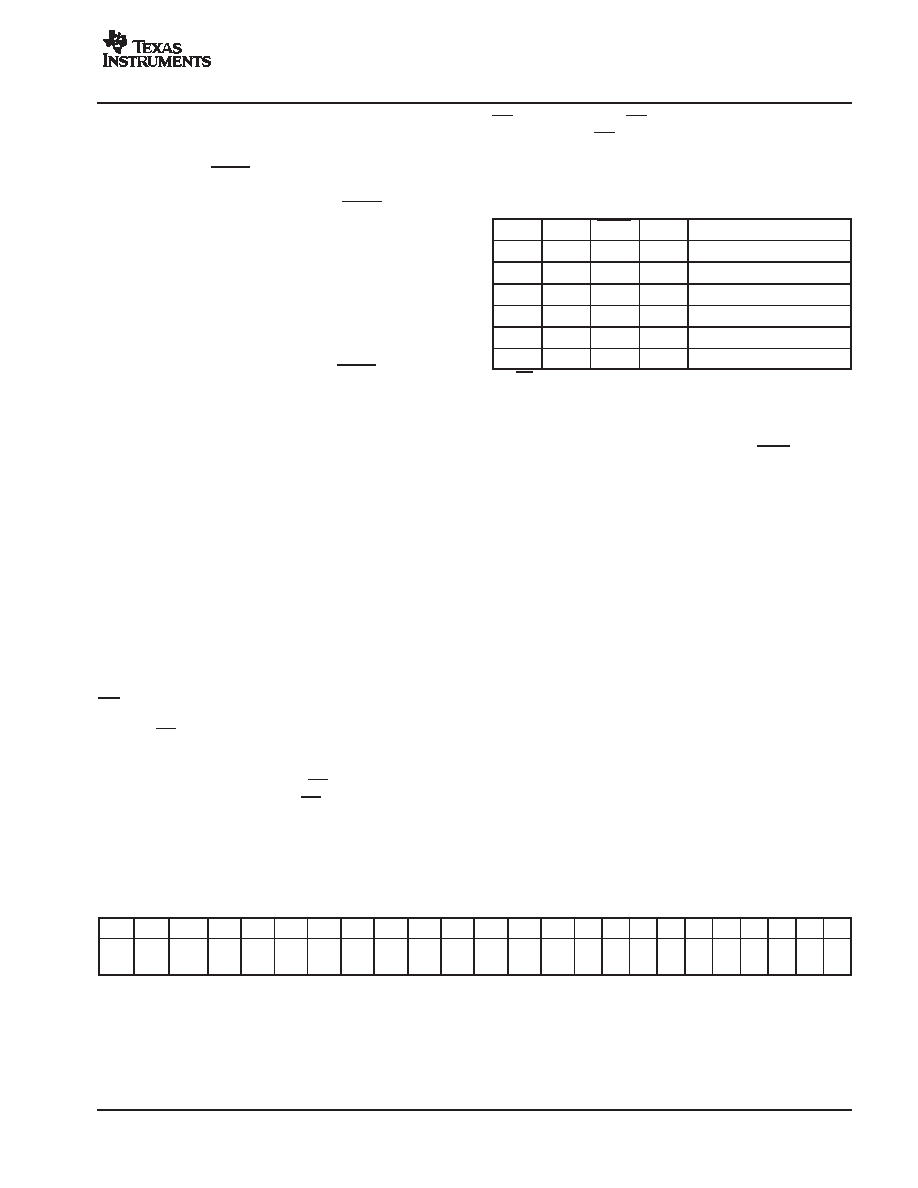
register. Table 2 shows more information.
Table 2. Serial Shift Register Truth Table
CS(1)
CLK(1)
LOAD
RST
SERIAL SHIFT REGISTER
H(2)
X(2)
H
No change
L(2)
L
H
No change
L
↑(2)
H
Advanced one bit
↑
L
H
Advanced one bit
H(3)
X
L(4)
H
No change
H(3)
X
H
↑(5)
No change
(1) CS and CLK are interchangeable.
(2) H = logic high. X = don’t care. L = logic low. ↑ = positive logic
transition.
(3) A high value is suggested in order to avoid a false clock from
advancing and changing the shift register.
(4) If data are clocked into the serial register while LOAD is low, the
selected DAC register will change as the shift register bits flow
through A1 and A0. This will corrupt the data in each DAC register
that has been erroneously selected.
(5) Rising edge of RST causes no change in the contents of the serial
shift register.
GLITCH SUPPRESSION CIRCUIT
Figure 21, Figure 22, Figure 48, and Figure 49 show the
typical DAC output when switching between codes 7FFFh
and 8000h. For R-2R ladder DACs, this is potentially the
worst-case glitch condition, since every switch in the DAC
changes state. To minimize the glitch energy at this and
other code pairs with possible high-glitch outputs, an
internal track-and-hold circuit is used to maintain the DAC
ouput voltage at a nearly constant level during the internal
switching interval. This track-and-hold circuit is activated
only when the transition is at, or close to, one of the code
pairs with the high-glitch possibility.
It is advisable to avoid digital transitions within 1
s of the
rising edge of the LDAC signal. These signals can affect
the
charge
on
the
track-and-hold
capacitor, thus
increasing the glitch energy.
Table 3. 24-Bit Data and Command Word
B23
B22
B21
B20
B19
B18
B17
B16
B15
B14
B13
B12
B11
B10
B9
B8
B7
B6
B5
B4
B3
B2
B1
B0
A1
A0
Quick
Load
X
D15
D14
D13
D12
D11
D10
D9
D8
D7
D6
D5
D4
D3
D2
D1
D0
相关PDF资料 |
PDF描述 |
|---|---|
| DAC7714U | QUAD, SERIAL INPUT LOADING, 8 us SETTLING TIME, 12-BIT DAC, PDSO16 |
| DAC7801LUG4 | PARALLEL, 8 BITS INPUT LOADING, 0.4 us SETTLING TIME, 12-BIT DAC, PDSO24 |
| DAC7800LU | SERIAL INPUT LOADING, 0.4 us SETTLING TIME, 12-BIT DAC, PDSO16 |
| DAC8228FSZ | DUAL, PARALLEL, 8 BITS INPUT LOADING, 2 us SETTLING TIME, 8-BIT DAC, PDSO20 |
| DAC8229FPZ | DUAL, PARALLEL, 8 BITS INPUT LOADING, 2 us SETTLING TIME, 8-BIT DAC, PDIP20 |
相关代理商/技术参数 |
参数描述 |
|---|---|
| DAC7664 | 制造商:TI 制造商全称:Texas Instruments 功能描述:16-BIT, QUAD VOLTAGE OUTPUT DIGITAL-TO-ANALOG CONVERTER |
| DAC7664YBR | 功能描述:数模转换器- DAC DAC Quad 16 Bit 12uS Settling Time RoHS:否 制造商:Texas Instruments 转换器数量:1 DAC 输出端数量:1 转换速率:2 MSPs 分辨率:16 bit 接口类型:QSPI, SPI, Serial (3-Wire, Microwire) 稳定时间:1 us 最大工作温度:+ 85 C 安装风格:SMD/SMT 封装 / 箱体:SOIC-14 封装:Tube |
| DAC7664YBRG4 | 功能描述:数模转换器- DAC DAC Quad 16 Bit 12uS Settling Time RoHS:否 制造商:Texas Instruments 转换器数量:1 DAC 输出端数量:1 转换速率:2 MSPs 分辨率:16 bit 接口类型:QSPI, SPI, Serial (3-Wire, Microwire) 稳定时间:1 us 最大工作温度:+ 85 C 安装风格:SMD/SMT 封装 / 箱体:SOIC-14 封装:Tube |
| DAC7664YBT | 功能描述:数模转换器- DAC DAC Quad 16 Bit 12uS Settling Time RoHS:否 制造商:Texas Instruments 转换器数量:1 DAC 输出端数量:1 转换速率:2 MSPs 分辨率:16 bit 接口类型:QSPI, SPI, Serial (3-Wire, Microwire) 稳定时间:1 us 最大工作温度:+ 85 C 安装风格:SMD/SMT 封装 / 箱体:SOIC-14 封装:Tube |
| DAC7664YBTG4 | 功能描述:数模转换器- DAC DAC Quad 16 Bit 12uS Settling Time RoHS:否 制造商:Texas Instruments 转换器数量:1 DAC 输出端数量:1 转换速率:2 MSPs 分辨率:16 bit 接口类型:QSPI, SPI, Serial (3-Wire, Microwire) 稳定时间:1 us 最大工作温度:+ 85 C 安装风格:SMD/SMT 封装 / 箱体:SOIC-14 封装:Tube |
发布紧急采购,3分钟左右您将得到回复。