- 您现在的位置:买卖IC网 > PDF目录10815 > DAC7802LU/1K (Texas Instruments)IC DUAL 12B CMOS MULT D/A 24SOIC PDF资料下载
参数资料
| 型号: | DAC7802LU/1K |
| 厂商: | Texas Instruments |
| 文件页数: | 23/23页 |
| 文件大小: | 0K |
| 描述: | IC DUAL 12B CMOS MULT D/A 24SOIC |
| 产品培训模块: | Data Converter Basics |
| 标准包装: | 1,000 |
| 设置时间: | 400ns |
| 位数: | 12 |
| 数据接口: | 并联 |
| 转换器数目: | 2 |
| 电压电源: | 单电源 |
| 工作温度: | -40°C ~ 85°C |
| 安装类型: | 表面贴装 |
| 封装/外壳: | 24-SOIC(0.295",7.50mm 宽) |
| 供应商设备封装: | 24-SOIC |
| 包装: | 带卷 (TR) |
| 输出数目和类型: | 2 电流,单极;2 电流,双极 |
DAC7800, 7801, 7802
9
SBAS005A
www.ti.com
DGND should be connected together at one point only,
preferably at the power-supply ground point. Separate re-
turns minimize current flow in low-level signal paths if properly
connected. Output op amp analog common (+ input) should
be connected as near to the AGND pins of the DAC780x as
possible.
WIRING PRECAUTIONS
To minimize AC feedthrough when designing a PC board,
care should be taken to minimize capacitive coupling be-
tween the VREF lines and the IOUT lines. Similarly, capacitive
coupling between DACs may compromise the channel-to-
channel isolation. Coupling from any of the digital control or
data lines might degrade the glitch and digital crosstalk
performance. Solder the DAC780x directly into the PC board
without a socket. Sockets add parasitic capacitance (which
can degrade AC performance).
AMPLIFIER OFFSET VOLTAGE
The output amplifier used with the DAC780x should have low
input offset voltage to preserve the transfer function linearity.
The voltage output of the amplifier has an error component
which is the offset voltage of the op amp multiplied by
the “noise gain” of the circuit. This “noise gain” is equal to
(RF/RO + 1) where RO is the output impedance of the DAC
IOUT terminal and RF is the feedback network impedance. The
nonlinearity occurs due to the output impedance varying with
code. If the 0 code case is excluded (where RO = infinity), the
RO will vary from R-3R providing a “noise gain” variation
between 4/3 and 2. In addition, the variation of RO is nonlinear
with code, and the largest steps in RO occur at major code
transitions where the worst differential nonlinearity is also
likely to be experienced. The nonlinearity seen at the amplifier
output is 2VOS – 4VOS/3 = 2VOS/3. Thus, to maintain good
nonlinearity the op amp offset should be much less than
1/2 LSB.
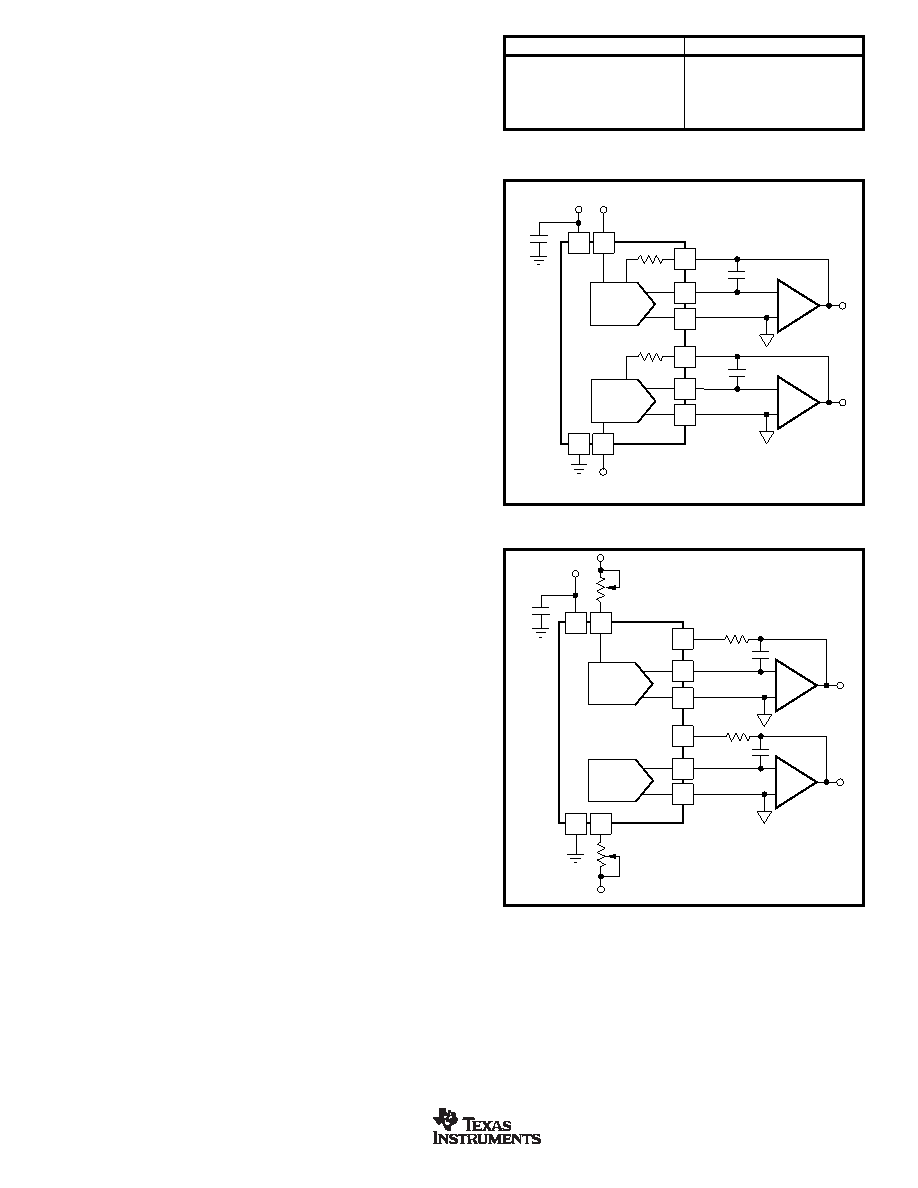
UNIPOLAR CONFIGURATION
Figure 3 shows DAC780x in a typical unipolar (two-quadrant)
multiplying configuration. The analog output values versus
digital input code are listed in Table II. The operational
amplifiers used in this circuit can be single amplifiers such as
the OPA602, or a dual amplifier such as the OPA2107. C1
and C2 provide phase compensation to minimize settling time
and overshoot when using a high speed operational amplifier.
If an application requires the DAC to have zero gain error, the
circuit shown in Figure 4 may be used. Resistors R2 and R4
induce a positive gain error greater than worst-case initial
negative gain error. Trim resistors R1 and R3 provide a
variable negative gain error and have sufficient trim range to
correct for the worst-case initial positive gain error plus the
error produced by R2 and R4.
BIPOLAR CONFIGURATION
See Figure 5 for the DAC780x in a typical bipolar (four-
quadrant) multiplying configuration. See Table III for the
listing of the analog output values versus digital input code.
DATA INPUT
ANALOG OUTPUT
MSB
↓↓ LSB
1111 1111 1111
–VREF (4095/4096)
1000 0000 0000
–VREF (2048/4096) = –1/2VREF
0000 0000 0001
–VREF (1/4096)
0000 0000 0000
0 Volts
TABLE II. Unipolar Output Code.
The operational amplifiers used in this circuit can be single
amplifiers such as the OPA602, a dual amplifier such as the
OPA2107, or a quad amplifier like the OPA404. C1 and C2
provide phase compensation to minimize settling time and
overshoot when using a high speed operational amplifier. The
bipolar offset resistors R5–R7 and R8–R10 should be ratio-
matched to 0.01% to ensure the specified gain error perfor-
mance.
DAC A
I
OUT A
DAC B
AGND A
I
OUT B
R
FB B
R
FB A
C1
10pF
C2
10pF
DAC780X
V
OUT A
V
OUT B
–
+
–
+
A1
A2
DGND
V
REF B
V
REF A
V
DD
+5V
C
D
A1, A2 OPA602 or 1/2 OPA2107.
DAC7802 has a single analog
common, AGND.
+
1F
AGND B
R
100
3
REF B
R
2
47
R
4
47
DAC A
I
OUT A
DAC B
AGND A
I
OUT B
R
FB B
R
FB A
C1 10pF
C2 10pF
DAC780X
V
OUT A
V
OUT B
–
+
–
+
A1
A2
DGND
V
DD
+5V
C
D
A1, A2 OPA602 or 1/2 OPA2107.
DAC7802 has a single analog
common, AGND.
+
1F
AGND B
V
IN A
R
100
1
REF A
V
IN B
V
FIGURE 4. Unipolar Configuration with Gain Trim.
FIGURE 3. Unipolar Configuration.
相关PDF资料 |
PDF描述 |
|---|---|
| VI-25N-CU-F3 | CONVERTER MOD DC/DC 18.5V 200W |
| ADM485JRZ | IC TX/RX SINGLE RS-485 5V 8SOIC |
| VI-25N-CU-F2 | CONVERTER MOD DC/DC 18.5V 200W |
| ADM1485JRZ | IC TX/RX RS-485 HS 5V 8SOIC |
| VI-25N-CU-F1 | CONVERTER MOD DC/DC 18.5V 200W |
相关代理商/技术参数 |
参数描述 |
|---|---|
| DAC7802LUG4 | 功能描述:数模转换器- DAC Dual Monolithic CMOS 12-Bit Multiplying RoHS:否 制造商:Texas Instruments 转换器数量:1 DAC 输出端数量:1 转换速率:2 MSPs 分辨率:16 bit 接口类型:QSPI, SPI, Serial (3-Wire, Microwire) 稳定时间:1 us 最大工作温度:+ 85 C 安装风格:SMD/SMT 封装 / 箱体:SOIC-14 封装:Tube |
| DAC7811 | 制造商:TI 制造商全称:Texas Instruments 功能描述:12-Bit, Serial Input, Multiplying Digital-to-Analog Converter |
| DAC7811EVM | 功能描述:数据转换 IC 开发工具 DAC7811 Eval Mod RoHS:否 制造商:Texas Instruments 产品:Demonstration Kits 类型:ADC 工具用于评估:ADS130E08 接口类型:SPI 工作电源电压:- 6 V to + 6 V |
| DAC7811IDGS | 功能描述:数模转换器- DAC 12-Bit Serial Input Multiplying DAC RoHS:否 制造商:Texas Instruments 转换器数量:1 DAC 输出端数量:1 转换速率:2 MSPs 分辨率:16 bit 接口类型:QSPI, SPI, Serial (3-Wire, Microwire) 稳定时间:1 us 最大工作温度:+ 85 C 安装风格:SMD/SMT 封装 / 箱体:SOIC-14 封装:Tube |
| DAC7811IDGSG4 | 功能描述:数模转换器- DAC 12-Bit Serial Input Multiplying DAC RoHS:否 制造商:Texas Instruments 转换器数量:1 DAC 输出端数量:1 转换速率:2 MSPs 分辨率:16 bit 接口类型:QSPI, SPI, Serial (3-Wire, Microwire) 稳定时间:1 us 最大工作温度:+ 85 C 安装风格:SMD/SMT 封装 / 箱体:SOIC-14 封装:Tube |
发布紧急采购,3分钟左右您将得到回复。