- 您现在的位置:买卖IC网 > PDF目录10805 > DAC8143FP (Analog Devices Inc)IC DAC 12BIT DAISY-CHAIN 16-DIP PDF资料下载
参数资料
| 型号: | DAC8143FP |
| 厂商: | Analog Devices Inc |
| 文件页数: | 11/12页 |
| 文件大小: | 0K |
| 描述: | IC DAC 12BIT DAISY-CHAIN 16-DIP |
| 产品培训模块: | Data Converter Fundamentals DAC Architectures |
| 产品变化通告: | Product Discontinuance 27/Oct/2011 |
| 标准包装: | 25 |
| 设置时间: | 380ns |
| 位数: | 12 |
| 数据接口: | 串行 |
| 转换器数目: | 1 |
| 电压电源: | 单电源 |
| 功率耗散(最大): | 500µW |
| 工作温度: | -40°C ~ 85°C |
| 安装类型: | 通孔 |
| 封装/外壳: | 16-DIP(0.300",7.62mm) |
| 供应商设备封装: | 16-PDIP |
| 包装: | 管件 |
| 输出数目和类型: | 2 电流,单极;2 电流,双极 |
| 采样率(每秒): | 2.63M |
DAC8143
–8–
REV. C
Where RO is a function of the digital code, and:
RO = 10 k for more than four bits of Logic 1,
RO = 30 k
for any single bit of Logic 1.
Therefore, the offset gain varies as follows:
at code 0011 1111 1111,
VERROR1 = VOS 1+
10 k
10 k
= 2 VOS
at code 0100 0000 0000,
VERROR2 = VOS 1+
10 k
30 k
= 4/3 VOS
The error difference is 2/3 VOS.
Since one LSB has a weight (for VREF = +10 V) of 2.4 mV for
the DAC8143, it is clearly important that VOS be minimized,
using either the amplifier’s pulling pins, an external pulling
network, or by selection of an amplifier with inherently low VOS.
Amplifiers with sufficiently low VOS include OP77, OP97, OP07,
OP27, and OP42.
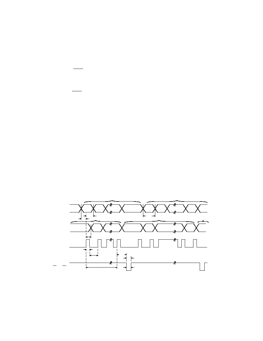
INTERFACE LOGIC OPERATION
The microprocessor interface of the DAC8143 has been design-
ed with multiple STROBE and LOAD inputs to maximize inter-
facing options. Control signals decoding may be done on chip or
with the use of external decoding circuitry (see Figure 21).
Serial data is clocked into the input register and buffered output
stage with STB1, STB2, or STB4. The strobe inputs are active
on the rising edge.
STB3 may be used with a falling edge clock
data.
WORD N
WORD N –1
WORD N –2
WORD N –1
WORD N
BIT 11
BIT 2
BIT 12
LSB
BIT 1
MSB
BIT 12
LSB
BIT 2
BIT 1
MSB
SRI
BIT 2
BIT 1
MSB
BIT 1
MSB
BIT 2
BIT 12
LSB
BIT 1
LSB
t
DS1, tDS2, tDS3, tDS4
SRO
t
DH1, tDH2, tDH3, tDH4
t
PD
t
STB1
t
STB2
t
STB3
t
STB4
tSTB1
tSTB2
tSTB3
tSTB4
* STROBE
(STB1, STB2, STB4)
12
1
2
t
LD1
t
LD2
t
SR1
12
11
t
ASB
LD1 AND LD2
LOAD NEW 12-BIT WORD INTO
INPUT REGISTER AND SHIFT
OUT PREVIOUS WORD
LOAD INPUT REGISTER'S
DATA INTO DAC REGISTER
NOTES:
* STROBE WAVEFORM IS INVERTED IF
STB
3 IS USED TO STROBE SERIAL DATA
BITS INTO INPUT REGISTER.
** DATA IS STROBED INTO AND OUT OF
THE INPUT SHIFT REGISTER MSB FIRST.
Figure 15. Timing Diagram
Serial data output (SRO) follows the serial data input (SRI) by
12 clocked bits.
Holding any STROBE input at its selected state (i.e., STB1,
STB2 or STB4 at logic HIGH or STB3 at logic LOW) will act to
prevent any further data input.
When a new data word has been entered into the input register,
it is transferred to the DAC register by asserting both LOAD
inputs.
The
CLR input allows asynchronous resetting of the DAC regis-
ter to 0000 0000 0000. This reset does not affect data held in
the input registers. While in unipolar mode, a CLEAR will
result in the analog output going to 0 V. In bipolar mode, the
output will go to –VREF.
INTERFACE INPUT DESCRIPTION
STB1 (Pin 4), STB2 (Pin 8), STB4 (Pin 11)—Input Register
and Buffered Output Strobe. Inputs Active on Rising
Edge. Selected to load serial data into input register and buff-
ered output stage. See Table I for details.
STB
3 (Pin 10)—Input Register and Buffered Output
Strobe Input. Active on Falling Edge. Selected to load serial
data into input register and buffered output stage. See Table I
for details.
LD
1 (Pin 5), LD2 (Pin 9)—Load DAC Register Inputs.
Active Low. Selected together to load contents of input register
into DAC register.
CLR (Pin 13)—Clear Input. Active Low. Asynchronous.
When LOW, 12-bit DAC register is forced to a zero code (0000
0000 0000) regardless of other interface inputs.
相关PDF资料 |
PDF描述 |
|---|---|
| VE-24N-CU-F2 | CONVERTER MOD DC/DC 18.5V 200W |
| VE-24M-CU-F2 | CONVERTER MOD DC/DC 10V 200W |
| ADM208ARSZ | IC TXRX RS-232 5V 0.1UF 24-SSOP |
| VE-24K-CU-F2 | CONVERTER MOD DC/DC 40V 200W |
| ADM207EARSZ | IC TXRX RS232 5DVR/3REC 24SSOP |
相关代理商/技术参数 |
参数描述 |
|---|---|
| DAC8143FPZ | 功能描述:IC DAC 12BIT DAISYCHAIN 16DIP RoHS:是 类别:集成电路 (IC) >> 数据采集 - 数模转换器 系列:- 产品培训模块:Data Converter Fundamentals DAC Architectures 标准包装:750 系列:- 设置时间:7µs 位数:16 数据接口:并联 转换器数目:1 电压电源:双 ± 功率耗散(最大):100mW 工作温度:0°C ~ 70°C 安装类型:表面贴装 封装/外壳:28-LCC(J 形引线) 供应商设备封装:28-PLCC(11.51x11.51) 包装:带卷 (TR) 输出数目和类型:1 电压,单极;1 电压,双极 采样率(每秒):143k |
| DAC8143FS | 功能描述:IC DAC 12BIT DAISY-CHAIN 16-SOIC RoHS:否 类别:集成电路 (IC) >> 数据采集 - 数模转换器 系列:- 标准包装:2,400 系列:- 设置时间:- 位数:18 数据接口:串行 转换器数目:3 电压电源:模拟和数字 功率耗散(最大):- 工作温度:-40°C ~ 85°C 安装类型:表面贴装 封装/外壳:36-TFBGA 供应商设备封装:36-TFBGA 包装:带卷 (TR) 输出数目和类型:* 采样率(每秒):* |
| DAC8143FS-REEL | 制造商:Analog Devices 功能描述:DAC 1-CH R-2R 12-bit 16-Pin SOIC W T/R |
| DAC8143FSZ | 功能描述:IC DAC 12BIT DAISY-CHAIN 16-SOIC RoHS:是 类别:集成电路 (IC) >> 数据采集 - 数模转换器 系列:- 产品培训模块:Lead (SnPb) Finish for COTS Obsolescence Mitigation Program 标准包装:50 系列:- 设置时间:4µs 位数:12 数据接口:串行 转换器数目:2 电压电源:单电源 功率耗散(最大):- 工作温度:-40°C ~ 85°C 安装类型:表面贴装 封装/外壳:8-TSSOP,8-MSOP(0.118",3.00mm 宽) 供应商设备封装:8-uMAX 包装:管件 输出数目和类型:2 电压,单极 采样率(每秒):* 产品目录页面:1398 (CN2011-ZH PDF) |
| DAC8143FSZ-REEL | 功能描述:IC DAC 12BIT DAISYCHAIN 16SOIC RoHS:是 类别:集成电路 (IC) >> 数据采集 - 数模转换器 系列:- 标准包装:47 系列:- 设置时间:2µs 位数:14 数据接口:并联 转换器数目:1 电压电源:单电源 功率耗散(最大):55µW 工作温度:-40°C ~ 85°C 安装类型:表面贴装 封装/外壳:28-SSOP(0.209",5.30mm 宽) 供应商设备封装:28-SSOP 包装:管件 输出数目和类型:1 电流,单极;1 电流,双极 采样率(每秒):* |
发布紧急采购,3分钟左右您将得到回复。