参数资料
| 型号: | DAC8143FPZ |
| 厂商: | Analog Devices Inc |
| 文件页数: | 10/12页 |
| 文件大小: | 0K |
| 描述: | IC DAC 12BIT DAISYCHAIN 16DIP |
| 产品培训模块: | Data Converter Fundamentals DAC Architectures |
| 标准包装: | 25 |
| 设置时间: | 380ns |
| 位数: | 12 |
| 数据接口: | 串行 |
| 转换器数目: | 1 |
| 电压电源: | 单电源 |
| 功率耗散(最大): | 500µW |
| 工作温度: | -40°C ~ 85°C |
| 安装类型: | 通孔 |
| 封装/外壳: | 16-DIP(0.300",7.62mm) |
| 供应商设备封装: | 16-PDIP |
| 包装: | 管件 |
| 输出数目和类型: | 2 电流,单极;2 电流,双极 |
| 采样率(每秒): | 2.63M |
DAC8143
–7–
REV. C
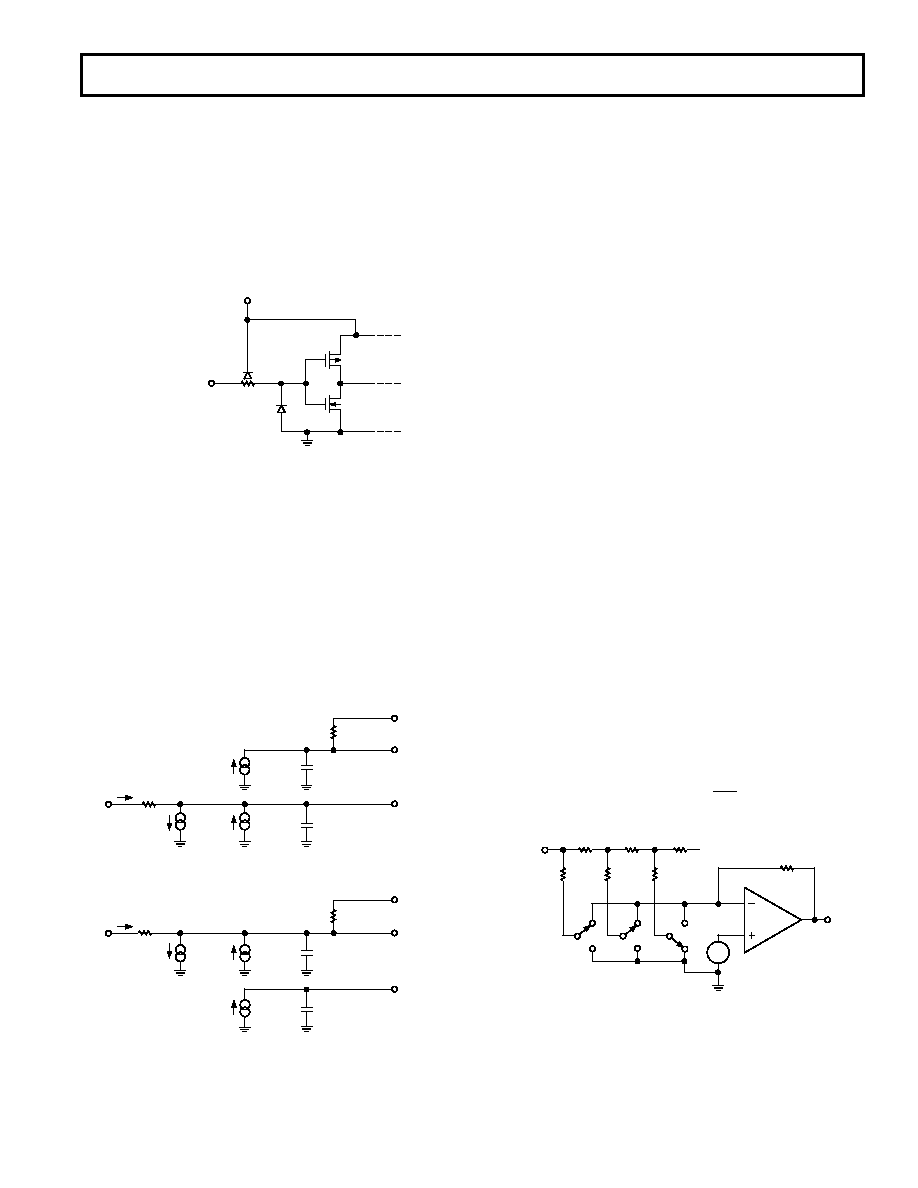
ESD PROTECTION
The DAC8143 digital inputs have been designed with ESD
resistance incorporated through careful layout and the inclusion
of input protection circuitry.
Figure 11 shows the input protection diodes. High voltage static
charges applied to the digital inputs are shunted to the supply
and ground rails through forward biased diodes.
These protection diodes were designed to clamp the inputs well
below dangerous levels during static discharge conditions.
VDD
DTL/TTL/CMOS
INPUTS
Figure 11. Digital Input Protection
EQUIVALENT CIRCUIT ANALYSIS
Figures 12 and 13 show equivalent circuits for the DAC8143’s
internal DAC with all bits LOW and HIGH, respectively. The
reference current is switched to IOUT2 when all data bits are LOW,
and to IOUT1 when all bits are HIGH. The ILEAKAGE current
source is the combination of surface and junction leakages to the
substrate. The 1/4096 current source represents the constant
1-bit current drain through the ladder’s terminating resistor.
Output capacitance is dependent upon the digital input code.
This is because the capacitance of a MOS transistor changes
with applied gate voltage. This output capacitance varies be-
tween the low and high values.
RFEEDBACK
IOUT1
IOUT2
R = 10k
ILEAKAGE
60pF
ILEAKAGE
90pF
1/4096
R = 10k
IREF
VREF
Figure 12. Equivalent Circuit (All Inputs LOW)
IOUT2
ILEAKAGE
60pF
RFEEDBACK
IOUT1
R = 10k
ILEAKAGE
90pF
1/4096
R = 10k
IREF
VREF
Figure 13. Equivalent Circuit (All Inputs HIGH)
DYNAMIC PERFORMANCE
ANALOG OUTPUT IMPEDANCE
The output resistance, as in the case of the output capacitance,
varies with the digital input code. This resistance, looking back
into the IOUT1 terminal, varies between 11 k (the feedback
resistor alone when all digital input are LOW) and 7.5 k
(the
feedback resistor in parallel with approximately 30 k
of the
R-2R ladder network resistance when any single bit logic is
HIGH). Static accuracy and dynamic performance will be af-
fected by these variations.
The gain and phase stability of the output amplifier, board
layout, and power supply decoupling will all affect the dynamic
performance of the DAC8143. The use of a small compensation
capacitor may be required when high speed operational amplifi-
ers are used. It may be connected across the amplifier’s feed-
back resistor to provide the necessary phase compensation to
critically damp the output.
The considerations when using high speed amplifiers are:
1. Phase compensation (see Figures 16 and 17).
2. Power supply decoupling at the device socket and use of
proper grounding techniques.
OUTPUT AMPLIFIER CONSIDERATIONS
When using high speed op amps, a small feedback capacitor
(typically 5 pF–30 pF) should be used across the amplifiers to
minimize overshoot and ringing. For low speed or static
applications, ac specifications of the amplifier are not very criti-
cal. In high speed applications, slew rate, settling time, open-
loop gain and gain/phase margin specifications of the amplifier
should be selected for the desired performance. It has already
been noted that an offset can be caused by including the usual
bias current compensation resistor in the amplifier’s noninvert-
ing input terminal. This resistor should not be used. Instead, the
amplifier should have a bias current that is low over the tem-
perature range of interest.
Static accuracy is affected by the variation in the DAC’s output
resistance. This variation is best illustrated by using the circuit
of Figure 14 and the equation:
VERROR = VOS 1+
RFB
RO
VOS
VREF
RR
R
ETC
RFB
R2
OP-77
Figure 14. Simplified Circuit
相关PDF资料 |
PDF描述 |
|---|---|
| DAC8228FSZ | IC DAC 8BIT DUAL V-OUT 20SOIC |
| DAC8512EP | IC DAC 12BIT SRL LP 5V 8-DIP |
| DAC8800FS | IC DAC 8BIT OCTAL CMOS 20-SOIC |
| DAC8841FS | IC DAC 8BIT OCTAL 2-QUAD 24-SOIC |
| DC-EM-02T-NC-25 | EM 8MB SDRAM 4MB FLASH SINGLE |
相关代理商/技术参数 |
参数描述 |
|---|---|
| DAC8143FS | 功能描述:IC DAC 12BIT DAISY-CHAIN 16-SOIC RoHS:否 类别:集成电路 (IC) >> 数据采集 - 数模转换器 系列:- 标准包装:2,400 系列:- 设置时间:- 位数:18 数据接口:串行 转换器数目:3 电压电源:模拟和数字 功率耗散(最大):- 工作温度:-40°C ~ 85°C 安装类型:表面贴装 封装/外壳:36-TFBGA 供应商设备封装:36-TFBGA 包装:带卷 (TR) 输出数目和类型:* 采样率(每秒):* |
| DAC8143FS-REEL | 制造商:Analog Devices 功能描述:DAC 1-CH R-2R 12-bit 16-Pin SOIC W T/R |
| DAC8143FSZ | 功能描述:IC DAC 12BIT DAISY-CHAIN 16-SOIC RoHS:是 类别:集成电路 (IC) >> 数据采集 - 数模转换器 系列:- 产品培训模块:Lead (SnPb) Finish for COTS Obsolescence Mitigation Program 标准包装:50 系列:- 设置时间:4µs 位数:12 数据接口:串行 转换器数目:2 电压电源:单电源 功率耗散(最大):- 工作温度:-40°C ~ 85°C 安装类型:表面贴装 封装/外壳:8-TSSOP,8-MSOP(0.118",3.00mm 宽) 供应商设备封装:8-uMAX 包装:管件 输出数目和类型:2 电压,单极 采样率(每秒):* 产品目录页面:1398 (CN2011-ZH PDF) |
| DAC8143FSZ-REEL | 功能描述:IC DAC 12BIT DAISYCHAIN 16SOIC RoHS:是 类别:集成电路 (IC) >> 数据采集 - 数模转换器 系列:- 标准包装:47 系列:- 设置时间:2µs 位数:14 数据接口:并联 转换器数目:1 电压电源:单电源 功率耗散(最大):55µW 工作温度:-40°C ~ 85°C 安装类型:表面贴装 封装/外壳:28-SSOP(0.209",5.30mm 宽) 供应商设备封装:28-SSOP 包装:管件 输出数目和类型:1 电流,单极;1 电流,双极 采样率(每秒):* |
| DAC8162 | 制造商:TI 制造商全称:Texas Instruments 功能描述:DUAL 16-/14-/12-BIT, ULTRALOW-GLITCH, LOW-POWER, BUFFERED, VOLTAGE-OUTPUT |
发布紧急采购,3分钟左右您将得到回复。