- 您现在的位置:买卖IC网 > PDF目录8575 > DAC8248FS-REEL (Analog Devices Inc)IC DAC 12BIT DUAL W/BUFF 24-SOIC PDF资料下载
参数资料
| 型号: | DAC8248FS-REEL |
| 厂商: | Analog Devices Inc |
| 文件页数: | 5/16页 |
| 文件大小: | 0K |
| 描述: | IC DAC 12BIT DUAL W/BUFF 24-SOIC |
| 产品培训模块: | Data Converter Fundamentals DAC Architectures |
| 标准包装: | 1,000 |
| 设置时间: | 1µs |
| 位数: | 12 |
| 数据接口: | 并联 |
| 转换器数目: | 2 |
| 电压电源: | 单电源 |
| 功率耗散(最大): | 50µW |
| 工作温度: | -40°C ~ 85°C |
| 安装类型: | 表面贴装 |
| 封装/外壳: | 24-SOIC(0.295",7.50mm 宽) |
| 供应商设备封装: | 24-SOIC W |
| 包装: | 带卷 (TR) |
| 输出数目和类型: | 2 电流,单极;2 电流,双极 |
| 采样率(每秒): | 1M |
DAC8248
–13–
REV. B
loading the appropriate DAC’s digital inputs with 0000 0000
0000 and adjusting the op amp’s offset voltage to 0 V. It is rec-
ommended that the op amp offset voltage be adjusted to less
than 10% of 1 LSB (244
V), and over the operating tempera-
ture range of interest. This will ensure the DAC’s monotonicity
and minimize gain and linearity errors.
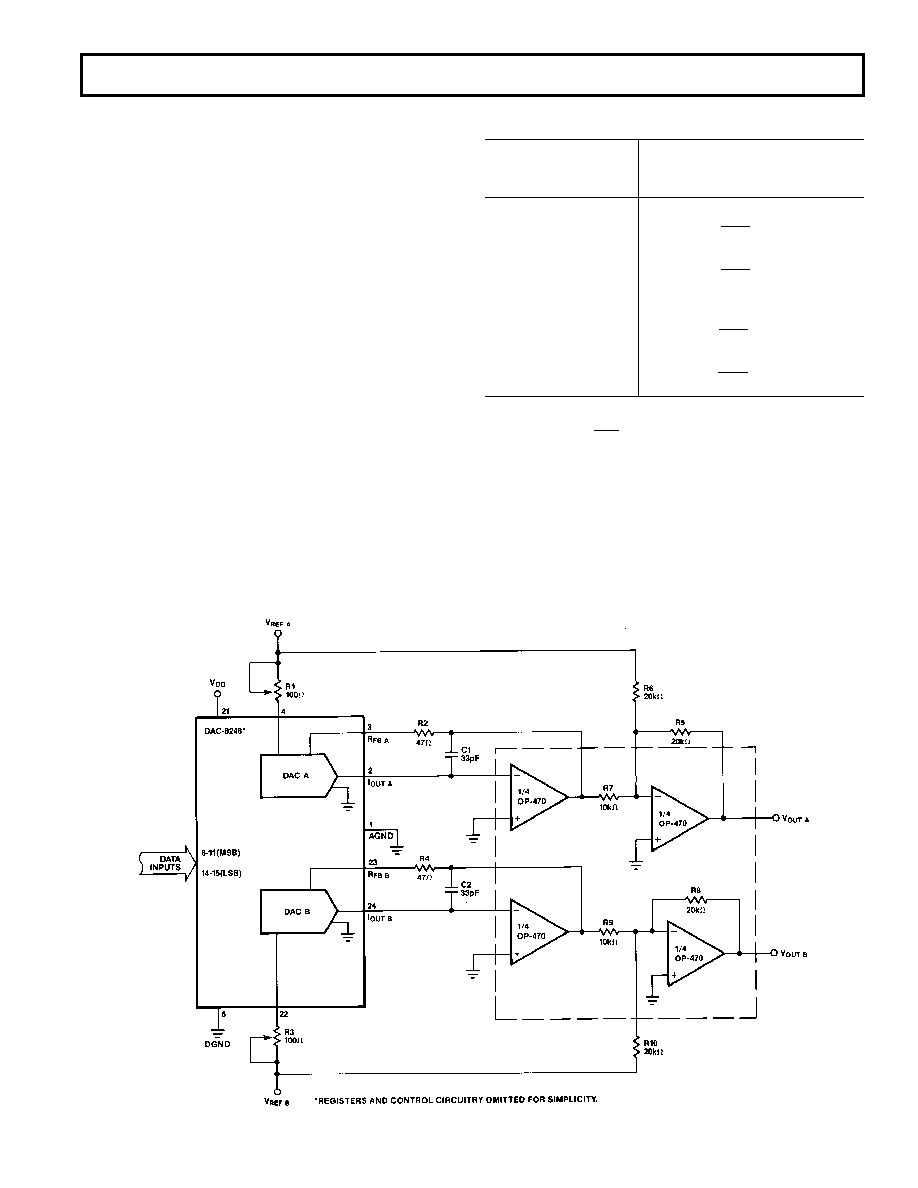
BIPOLAR OPERATION
The bipolar (offset binary) 4-quadrant configuration using the
DAC8248 is shown in Figure 8, and the corresponding code is
shown in Table II. The circuit makes use of the OP470, a quad
op amp (use four OP42s for applications requiring higher
speeds).
The full-scale output voltage may be adjusted by varying VREF or
the value of R5 and R8, and thus eliminating resistors R1, R2,
R3, and R4. If resistors R1 through R4 are omitted, then R5, R6,
R7 (R8, R9, and R10 for DAC B) should be ratio-matched to
0.01% to keep gain error within data sheet specifications. The re-
sistors should have identical temperature-coefficients if operating
over the full temperature range.
Zero and full-scale are adjusted in one of two ways and are at
the users discretion. Zero-output is adjusted by loading the ap-
propriate DAC’s digital inputs with 1000 0000 0000 and vary-
ing R1 (R3 for DAC B) so that VOUT A (or VOUT B) equals 0 V.
If R1, R2 (R3, R4 for DAC B) are omitted, then zero output
can be adjusted by varying R6, R7 ratios (R9, R10 for DAC B).
Full-scale is adjusted by loading the appropriate DAC’s digital
inputs with 1111 1111 1111 and varying R5 (R8 for DAC B).
Table II. Bipolar (Offset Binary) Code Table
(Refer to Figure 8)
Binary Number in
DAC Register
Analog Output, VOUT
MSB
LSB
(DAC A or DAC B)
1111 1111 1111
+VREF
2047
2048
1000 0000 0001
+VREF
1
2048
1000 0000 0000
0 V
0111 1111 1111
–VREF
1
2048
0000 0000 0000
–VREF
2048
NOTE:
1 LSB=(2
–11)(V
REF) =
1
2048
(VREF)
SINGLE SUPPLY OPERATION
CURRENT STEERING MODE
Because the DAC8248’s R-2R resistor ladder terminating resis-
tor is internally connected to AGND, it lends itself well for
single supply operation in the current steering mode configura-
tion. This means that AGND can be raised above system
Figure 8. Bipolar Configuration (4-Quadrant Multiplication)
相关PDF资料 |
PDF描述 |
|---|---|
| LTC1597ACG#TRPBF | IC D/A CONV 16BIT PAR 28-SSOP |
| LTC1597-1ACG#TRPBF | IC D/A CONV 16BIT PAR 28-SSOP |
| AD7225KPZ | IC DAC 8BIT QUAD W/AMP 28-PLCC |
| AD7537KN | IC DAC 12BIT LC2MOS DUAL 24-DIP |
| LTC2757BCLX#PBF | IC DAC 18BIT PAR 48LQFP |
相关代理商/技术参数 |
参数描述 |
|---|---|
| DAC8248FSZ | 功能描述:IC DAC 12BIT DUAL W/BUFF 24SOIC RoHS:是 类别:集成电路 (IC) >> 数据采集 - 数模转换器 系列:- 标准包装:1 系列:- 设置时间:4.5µs 位数:12 数据接口:串行,SPI? 转换器数目:1 电压电源:单电源 功率耗散(最大):- 工作温度:-40°C ~ 125°C 安装类型:表面贴装 封装/外壳:8-SOIC(0.154",3.90mm 宽) 供应商设备封装:8-SOICN 包装:剪切带 (CT) 输出数目和类型:1 电压,单极;1 电压,双极 采样率(每秒):* 其它名称:MCP4921T-E/SNCTMCP4921T-E/SNRCTMCP4921T-E/SNRCT-ND |
| DAC8248FSZ-REEL | 功能描述:IC DAC 12BIT DUAL W/BUFF 24SOIC RoHS:是 类别:集成电路 (IC) >> 数据采集 - 数模转换器 系列:- 产品培训模块:Data Converter Fundamentals DAC Architectures 标准包装:750 系列:- 设置时间:7µs 位数:16 数据接口:并联 转换器数目:1 电压电源:双 ± 功率耗散(最大):100mW 工作温度:0°C ~ 70°C 安装类型:表面贴装 封装/外壳:28-LCC(J 形引线) 供应商设备封装:28-PLCC(11.51x11.51) 包装:带卷 (TR) 输出数目和类型:1 电压,单极;1 电压,双极 采样率(每秒):143k |
| DAC8248FW | 制造商:Analog Devices 功能描述: |
| DAC8248GBC | 制造商:未知厂家 制造商全称:未知厂家 功能描述:12-Bit Digital-to-Analog Converter |
| DAC8248GP | 制造商:AD 制造商全称:Analog Devices 功能描述:Dual 12-Bit 8-Bit Byte Double-Buffered CMOS D/A Converter |
发布紧急采购,3分钟左右您将得到回复。