- 您现在的位置:买卖IC网 > PDF目录376563 > DAC8408FP (PRECISION MONOLITHICS INC) Quad 8-Bit Multiplying CMOS D/A Converter with Memory PDF资料下载
参数资料
| 型号: | DAC8408FP |
| 厂商: | PRECISION MONOLITHICS INC |
| 元件分类: | DAC |
| 英文描述: | Quad 8-Bit Multiplying CMOS D/A Converter with Memory |
| 中文描述: | 8-BIT DAC, PDIP28 |
| 文件页数: | 3/16页 |
| 文件大小: | 217K |
| 代理商: | DAC8408FP |
REV. A
–3–
DAC8408
@ V
DD
= +5 V; V
REF
=
6
10 V; V
OUT
A, B, C, D = 0 V; T
A
= –55
8
C to +125
8
C apply for
DAC8408AT/BT, T
A
= –40
8
C to +85
8
C apply for DAC8408ET/FT/FP/FPC/FS; T
A
= 0
8
C to +70
8
C apply for DAC8408GP, unless otherwse noted.
Specifications apply for DAC A, B, C, & D. Continued
ELECTRICAL CHARACTERISTICS
DAC8408
Min
Parameter
Symbol
Conditions
T yp
Max
Units
POWER SUPPLY
Voltage Range
Supply Current
8
Supply Current
9
V
DD
I
DD
I
DD
4.5
5.5
50
1.0
1.5
V
μ
A
mA
mA
T
A
= +25
°
C
T
A
= Full T emperature Range
NOT ES
1
T his is an end-point linearity specification.
2
Guaranteed to be monotonic over the full operating temperature range.
3
ppm/
°
C of FSR (FSR = Full Scale Range = V
-1 LSB.)
4
Input Resistance T emperature Coefficient = +300ppm/
°
C.
5
Logic Inputs are MOS gates. T ypical input current at +25
°
C Is less than 10 nA.
6
Guaranteed by design.
7
From Digital Input to 90% of final analog output current.
8
All Digital Inputs “0” or V
DD
.
9
All Digital Inputs V
IH
or V
IL
.
10
See T iming Diagram.
11
Digital Inputs = 0 V to V
DD
or V
DD
to 0 V.
12
Extrapolated: t
S
(1/2 LSB) = t
PD
+ 6.2
τ
where
τ
= the measured first time con-
stant of the final RC decay.
13
All Digital Inputs = 0 V; V
REF
= +10 V.
Specifications subject to change without notice.
Package T ype
u
JA
*
u
JC
Units
28-Pin Hermetic DIP (T )
28-Pin Plastic DIP (P)
28-Pin SOL (S)
28-Contact PLCC (PC)
55
53
68
66
10
27
23
29
°
C/W
°
C/W
°
C/W
°
C/W
*
θ
JA
is specified for worst case mounting conditions, i.e.,
θ
JA
is specified for
device in socket for cerdip and P-DIP packages;
θ
JA
is specified for device
soldered to printed circuit board for SOL and PLCC packages.
C AUT ION
1. Do not apply voltages higher than V
DD
+0.3 V or less than
–0.3 V potential on any terminal except V
REF
and R
FB
.
2. T he digital control inputs are diode-protected; however,
permanent damage may occur on unconnected inputs from
high energy electrostatic fields. K eep in conductive foam at
all times until ready to use.
3. Use proper antistatic handling procedures.
4. Absolute Maximum Ratings apply to both packaged devices
and DICE. Stresses above those listed under Absolute Maxi-
mum Ratings may cause permanent damage to the device.
ABSOLUT E MAX IMUM RAT INGS
(T
A
= +25
°
C, unless otherwise noted.)
V
DD
to I
OUT
2A
, I
OUT
2B
, I
OUT
2C
, I
OUT
2D
. . . . . . . . . .0 V, +7 V
V
DD
to DGND . . . . . . . . . . . . . . . . . . . . . . . . . . . . . .0 V, +7 V
I
OUT
1A
, I
OUT
1B
,
I
OUT 1C
, I
OUT 1D
to DGND . . . . . . . . . –0.3 V to V
DD
+0.3 V
R
FB
A, R
FB
B, R
FB
C, R
FB
D to I
OUT
. . . . . . . . . . . . . . . . .
±
25 V
I
OUT 2A
, I
OUT 2B
,
I
OUT 2C
, I
OUT 2D
to DGND . . . . . . . . . –0.3 V to V
DD
+ 0.3 V
DB0 through DB7 to DGND . . . . . . . . –0.3 V to V
DD
+ 0.3 V
Control Logic
Input Voltage to DGND . . . . . . . . . . –0.3 V + V
DD
+ 0.3 V
V
REF
A, V
REF
B, V
REF
C, V
REF
D to
I
OUT 2A
, I
OUT 2B
, I
OUT 2C
, I
OUT 2D
Operating T emperature Range
Commercial Grade (GP) . . . . . . . . . . . . . . . . 0
°
C to +70
°
C
Industrial Grade (ET , FT , FP, FPC, FS) . –40
°
C to +85
°
C
Military Grade (AT , BT ) . . . . . . . . . . . . . .–55
°
C to +125
°
C
Junction T emperature . . . . . . . . . . . . . . . . . . . . . . . . . +150
°
C
Storage T emperature . . . . . . . . . . . . . . . . . . .–65
°
C to +150
°
C
Lead T emperature (Soldering, 10 sec) . . . . . . . . . . . . . +300
°
C
. . . . . . . . . . . . . . . .
±
25 V
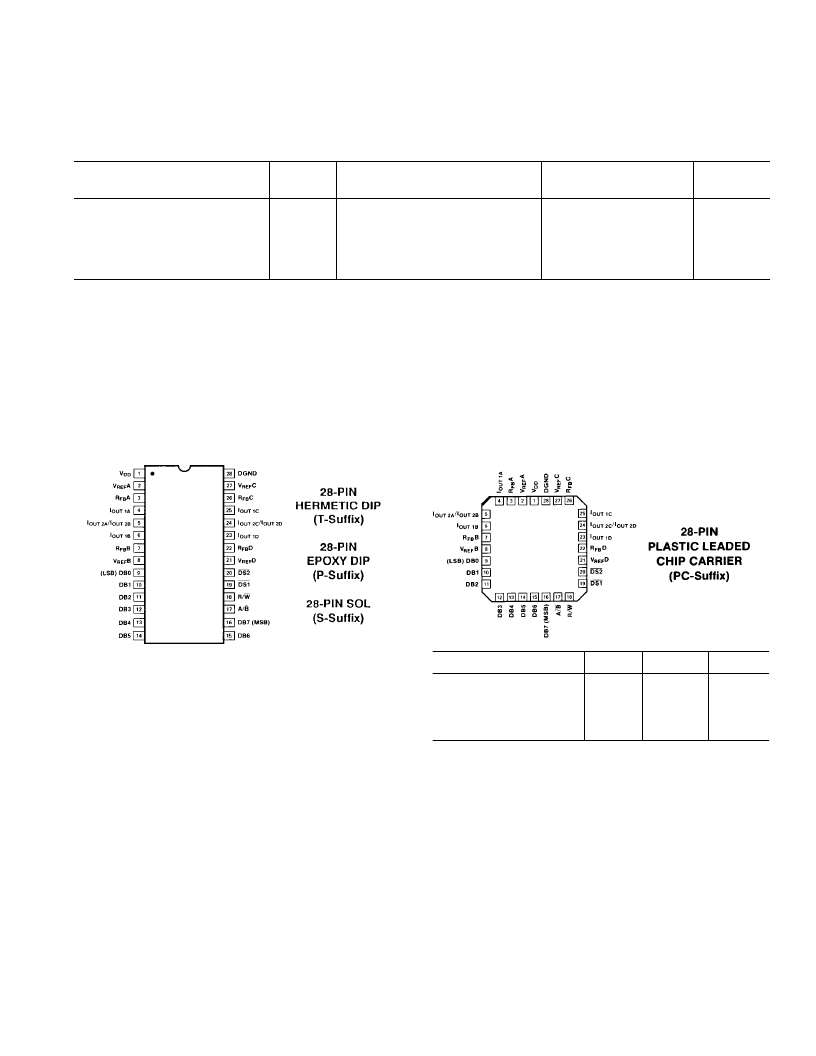
PIN CONNE CT IONS
DAC8408
TOP VIEW
(Not to Scale)
相关PDF资料 |
PDF描述 |
|---|---|
| DAC8408FPC | Quad 8-Bit Multiplying CMOS D/A Converter with Memory |
| DAC8408FS | Quad 8-Bit Multiplying CMOS D/A Converter with Memory |
| DAC8408FT | Quad 8-Bit Multiplying CMOS D/A Converter with Memory |
| DAC8408GP | Quad 8-Bit Multiplying CMOS D/A Converter with Memory |
| DAC8412FTC | 12-Bit Digital-to-Analog Converter |
相关代理商/技术参数 |
参数描述 |
|---|---|
| DAC8408FPC | 功能描述:IC DAC 8BIT QUAD W/MEMORY 28PLCC RoHS:否 类别:集成电路 (IC) >> 数据采集 - 数模转换器 系列:- 产品培训模块:Data Converter Fundamentals DAC Architectures 标准包装:750 系列:- 设置时间:7µs 位数:16 数据接口:并联 转换器数目:1 电压电源:双 ± 功率耗散(最大):100mW 工作温度:0°C ~ 70°C 安装类型:表面贴装 封装/外壳:28-LCC(J 形引线) 供应商设备封装:28-PLCC(11.51x11.51) 包装:带卷 (TR) 输出数目和类型:1 电压,单极;1 电压,双极 采样率(每秒):143k |
| DAC8408FPC3 | 制造商:AD 制造商全称:Analog Devices 功能描述:Quad 8-Bit Multiplying CMOS D/A Converter with Memory |
| DAC8408FPCZ | 功能描述:IC DAC 8BIT QUAD MULTIPLY 28PLCC RoHS:是 类别:集成电路 (IC) >> 数据采集 - 数模转换器 系列:- 产品培训模块:Data Converter Fundamentals DAC Architectures 标准包装:750 系列:- 设置时间:7µs 位数:16 数据接口:并联 转换器数目:1 电压电源:双 ± 功率耗散(最大):100mW 工作温度:0°C ~ 70°C 安装类型:表面贴装 封装/外壳:28-LCC(J 形引线) 供应商设备封装:28-PLCC(11.51x11.51) 包装:带卷 (TR) 输出数目和类型:1 电压,单极;1 电压,双极 采样率(每秒):143k |
| DAC8408FPZ | 功能描述:IC DAC 8BIT QUAD W/MEMORY 28DIP RoHS:是 类别:集成电路 (IC) >> 数据采集 - 数模转换器 系列:- 标准包装:1 系列:- 设置时间:4.5µs 位数:12 数据接口:串行,SPI? 转换器数目:1 电压电源:单电源 功率耗散(最大):- 工作温度:-40°C ~ 125°C 安装类型:表面贴装 封装/外壳:8-SOIC(0.154",3.90mm 宽) 供应商设备封装:8-SOICN 包装:剪切带 (CT) 输出数目和类型:1 电压,单极;1 电压,双极 采样率(每秒):* 其它名称:MCP4921T-E/SNCTMCP4921T-E/SNRCTMCP4921T-E/SNRCT-ND |
| DAC8408FS | 功能描述:IC DAC 8BIT QUAD W/MEMORY 28SOIC RoHS:否 类别:集成电路 (IC) >> 数据采集 - 数模转换器 系列:- 产品培训模块:Data Converter Fundamentals DAC Architectures 标准包装:750 系列:- 设置时间:7µs 位数:16 数据接口:并联 转换器数目:1 电压电源:双 ± 功率耗散(最大):100mW 工作温度:0°C ~ 70°C 安装类型:表面贴装 封装/外壳:28-LCC(J 形引线) 供应商设备封装:28-PLCC(11.51x11.51) 包装:带卷 (TR) 输出数目和类型:1 电压,单极;1 电压,双极 采样率(每秒):143k |
发布紧急采购,3分钟左右您将得到回复。