参数资料
| 型号: | DAC8408FPZ |
| 厂商: | Analog Devices Inc |
| 文件页数: | 10/16页 |
| 文件大小: | 0K |
| 描述: | IC DAC 8BIT QUAD W/MEMORY 28DIP |
| 产品培训模块: | Data Converter Fundamentals DAC Architectures |
| 标准包装: | 13 |
| 设置时间: | 190ns |
| 位数: | 8 |
| 数据接口: | 并联 |
| 转换器数目: | 4 |
| 电压电源: | 单电源 |
| 工作温度: | -40°C ~ 85°C |
| 安装类型: | 通孔 |
| 封装/外壳: | 28-DIP(0.600",15.24mm) |
| 供应商设备封装: | 28-PDIP |
| 包装: | 管件 |
| 输出数目和类型: | 4 电流,单极;4 电流,双极 |
| 采样率(每秒): | 5.26M |
REV. A
–3–
DAC8408
@ VDD = +5 V; VREF =
10 V; VOUTA, B, C, D = 0 V; TA = –55 C to +125 C apply for
DAC8408AT/BT, TA = –40 C to +85 C apply for DAC8408ET/FT/FP/FPC/FS; TA = 0 C to +70 C apply for DAC8408GP, unless otherwise noted.
Specifications apply for DAC A, B, C, & D.
Continued
ELECTRICAL CHARACTERISTICS
DAC8408
Parameter
Symbol
Conditions
Min
Typ
Max
Units
POWER SUPPLY
Voltage Range
VDD
4.5
5.5
V
Supply Current8
IDD
50
A
Supply Current
9
IDD
TA = +25
°C
1.0
mA
TA = Full Temperature Range
1.5
mA
NOTES
1This is an end-point linearity specification.
2Guaranteed to be monotonic over the full operating temperature range.
3ppm/
°C of FSR (FSR = Full Scale Range = V
REF-1 LSB.)
4Input Resistance Temperature Coefficient = +300ppm/
°C.
5Logic Inputs are MOS gates. Typical input current at +25
°C Is less than 10 nA.
6Guaranteed by design.
7From Digital Input to 90% of final analog output current.
8All Digital Inputs “0” or V
DD.
9All Digital Inputs V
IH or VIL.
10See Timing Diagram.
11Digital Inputs = 0 V to V
DD or VDD to 0 V.
12Extrapolated: t
S (1/2 LSB) = tPD + 6.2τ where τ = the measured first time con-
stant of the final RC decay.
13All Digital Inputs = 0 V; V
REF = +10 V.
Specifications subject to change without notice.
Package Type
JA*
JC
Units
28-Pin Hermetic DIP (T)
55
10
°C/W
28-Pin Plastic DIP (P)
53
27
°C/W
28-Pin SOL (S)
68
23
°C/W
28-Contact PLCC (PC)
66
29
°C/W
*
θ
JA is specified for worst case mounting conditions, i.e., θJA is specified for
device in socket for cerdip and P-DIP packages;
θ
JA is specified for device
soldered to printed circuit board for SOL and PLCC packages.
CAUTION
1. Do not apply voltages higher than VDD +0.3 V or less than
–0.3 V potential on any terminal except VREF and RFB.
2. The digital control inputs are diode-protected; however,
permanent damage may occur on unconnected inputs from
high energy electrostatic fields. Keep in conductive foam at
all times until ready to use.
3. Use proper antistatic handling procedures.
4. Absolute Maximum Ratings apply to both packaged devices
and DICE. Stresses above those listed under Absolute Maxi-
mum Ratings may cause permanent damage to the device.
ABSOLUTE MAXIMUM RATINGS
(TA = +25
°C, unless otherwise noted.)
VDD to IOUT 2A, IOUT 2B, IOUT 2C, IOUT 2D . . . . . . . . . . 0 V, +7 V
VDD to DGND . . . . . . . . . . . . . . . . . . . . . . . . . . . . . . 0 V, +7 V
IOUT 1A, IOUT 1B,
IOUT 1C, IOUT 1D to DGND . . . . . . . . . –0.3 V to VDD +0.3 V
RFBA, RFBB, RFBC, RFBD to IOUT . . . . . . . . . . . . . . . . .
±25 V
IOUT 2A, IOUT 2B,
IOUT 2C, IOUT 2D to DGND . . . . . . . . . –0.3 V to VDD + 0.3 V
DB0 through DB7 to DGND . . . . . . . . –0.3 V to VDD + 0.3 V
Control Logic
Input Voltage to DGND . . . . . . . . . . –0.3 V + VDD + 0.3 V
VREFA, VREFB, VREFC, VREFD to
IOUT 2A, IOUT 2B, IOUT 2C, IOUT 2D
. . . . . . . . . . . . . . . .
±25 V
Operating Temperature Range
Commercial Grade (GP) . . . . . . . . . . . . . . . . 0
°C to +70°C
Industrial Grade (ET, FT, FP, FPC, FS) . –40
°C to +85°C
Military Grade (AT, BT) . . . . . . . . . . . . . . –55
°C to +125°C
Junction Temperature . . . . . . . . . . . . . . . . . . . . . . . . . +150
°C
Storage Temperature . . . . . . . . . . . . . . . . . . . –65
°C to +150°C
Lead Temperature (Soldering, 10 sec) . . . . . . . . . . . . . +300
°C
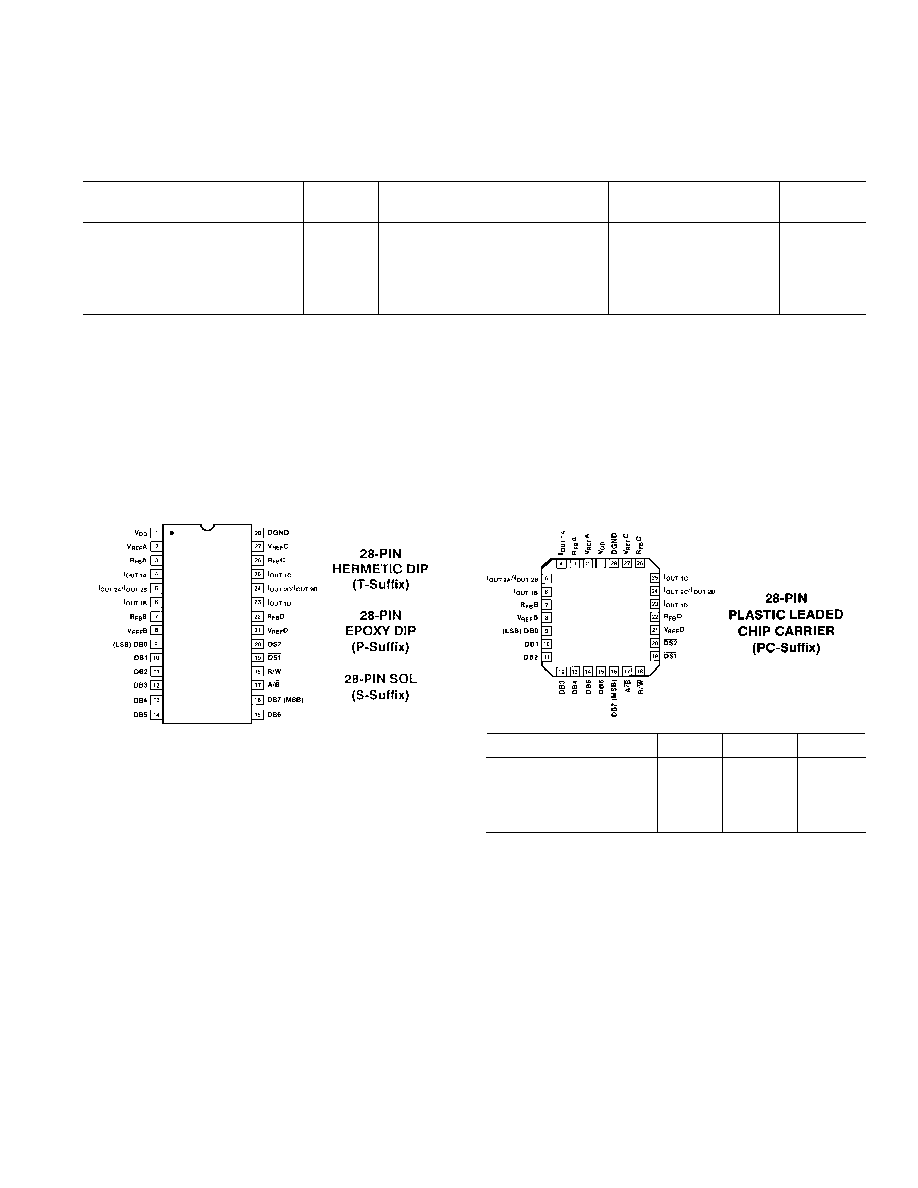
PIN CONNECTIONS
DAC8408
TOP VIEW
(Not to Scale)
相关PDF资料 |
PDF描述 |
|---|---|
| VI-21B-MW-F3 | CONVERTER MOD DC/DC 95V 100W |
| MS27473T16B26BA | CONN HSG PLUG 26POS STRGHT SCKT |
| AD9716BCPZ | IC DAC DUAL 12BIT LO PWR 40LFCSP |
| MS27656T11B5SLC | CONN HSG RCPT 5POS WALL MT SCKT |
| VI-21B-MW-F2 | CONVERTER MOD DC/DC 95V 100W |
相关代理商/技术参数 |
参数描述 |
|---|---|
| DAC8408FS | 功能描述:IC DAC 8BIT QUAD W/MEMORY 28SOIC RoHS:否 类别:集成电路 (IC) >> 数据采集 - 数模转换器 系列:- 产品培训模块:Data Converter Fundamentals DAC Architectures 标准包装:750 系列:- 设置时间:7µs 位数:16 数据接口:并联 转换器数目:1 电压电源:双 ± 功率耗散(最大):100mW 工作温度:0°C ~ 70°C 安装类型:表面贴装 封装/外壳:28-LCC(J 形引线) 供应商设备封装:28-PLCC(11.51x11.51) 包装:带卷 (TR) 输出数目和类型:1 电压,单极;1 电压,双极 采样率(每秒):143k |
| DAC8408FS-REEL | 制造商:Analog Devices 功能描述:DAC 4-CH R-2R 8-bit 28-Pin SOIC W T/R 制造商:Analog Devices 功能描述:DAC8408 W/TAPE & REEL - Tape and Reel 制造商:Rochester Electronics LLC 功能描述:DAC8408 W/TAPE & REEL - Tape and Reel |
| DAC8408FSZ | 功能描述:IC DAC 8BIT QUAD W/MEMORY 28SOIC RoHS:是 类别:集成电路 (IC) >> 数据采集 - 数模转换器 系列:- 标准包装:1 系列:- 设置时间:4.5µs 位数:12 数据接口:串行,SPI? 转换器数目:1 电压电源:单电源 功率耗散(最大):- 工作温度:-40°C ~ 125°C 安装类型:表面贴装 封装/外壳:8-SOIC(0.154",3.90mm 宽) 供应商设备封装:8-SOICN 包装:剪切带 (CT) 输出数目和类型:1 电压,单极;1 电压,双极 采样率(每秒):* 其它名称:MCP4921T-E/SNCTMCP4921T-E/SNRCTMCP4921T-E/SNRCT-ND |
| DAC8408FSZ | 制造商:Analog Devices 功能描述:IC 8-BIT DAC |
| DAC8408FSZ-REEL | 功能描述:IC DAC 8BIT QUAD W/MEMORY 28SOIC RoHS:是 类别:集成电路 (IC) >> 数据采集 - 数模转换器 系列:- 标准包装:47 系列:- 设置时间:2µs 位数:14 数据接口:并联 转换器数目:1 电压电源:单电源 功率耗散(最大):55µW 工作温度:-40°C ~ 85°C 安装类型:表面贴装 封装/外壳:28-SSOP(0.209",5.30mm 宽) 供应商设备封装:28-SSOP 包装:管件 输出数目和类型:1 电流,单极;1 电流,双极 采样率(每秒):* |
发布紧急采购,3分钟左右您将得到回复。