参数资料
| 型号: | DAC8408FS |
| 厂商: | Analog Devices Inc |
| 文件页数: | 15/16页 |
| 文件大小: | 0K |
| 描述: | IC DAC 8BIT QUAD W/MEMORY 28SOIC |
| 产品培训模块: | Data Converter Fundamentals DAC Architectures |
| 标准包装: | 27 |
| 设置时间: | 190ns |
| 位数: | 8 |
| 数据接口: | 并联 |
| 转换器数目: | 4 |
| 电压电源: | 单电源 |
| 工作温度: | -40°C ~ 85°C |
| 安装类型: | 表面贴装 |
| 封装/外壳: | 28-SOIC(0.295",7.50mm 宽) |
| 供应商设备封装: | 28-SOIC W |
| 包装: | 管件 |
| 输出数目和类型: | 4 电流,单极;4 电流,双极 |
| 采样率(每秒): | 5.26M |
DAC8408
–8–
REV. A
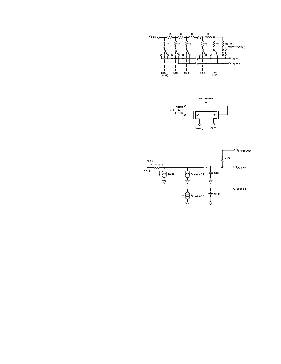
CIRCUIT INFORMATION
The DAC8408 combines four identical 8-bit CMOS DACs
onto a single monolithic chip. Each DAC has its own reference
input, feedback resistor, and on-board data latches. It also fea-
tures a read/write function that serves as an accessible memory
location for digital-input data words. The DAC’s three-state
readback drivers place the data word back onto the data bus.
D/A CONVERTER SECTION
Each DAC contains a highly stable, silicon-chromium, thin-film,
R-2R resistor ladder network and eight pairs of current steering
switches. These switches are in series with each ladder resistor
and are single-pole, double-throw NMOS transistors; the gates
of these transistors are controlled by CMOS inverters. Figure 1
shows a simplified circuit of the R-2R resistor ladder section,
and Figure 2 shows an approximate equivalent switch circuit.
The current through each resistor leg is switched between IOUT 1
and IOUT 2. This maintains a constant current in each leg, re-
gardless of the digital input logic states.
Each transistor switch has a finite “ON” resistance that can in-
troduce errors to the DAC’s specified performance. These resis-
tances must be accounted for by making the voltage drop across
each transistor equal to each other. This is done by binarily-
scaling the transistor’s “ON” resistance from the most signifi-
cant bit (MSB) to the least significant bit (LSB). With 10 volts
applied at the reference input, the current through the MSB
switch is 0.5 mA, the next bit is 0.25 mA, etc.; this maintains a
constant 10 mV drop across each switch and the converter’s ac-
curacy is maintained. It also results in a constant resistance ap-
pearing at the DAC’s reference input terminal; this allows the
DAC to be driven by a voltage or current source, ac or dc of
positive or negative polarity.
Shown in Figure 3 is an equivalent output circuit for DAC A.
The circuit is shown with all digital inputs high. The leakage
current source is the combination of surface and junction leak-
ages to the substrate. The 1/256 current source represents the
constant 1-bit current drain through the ladder terminating re-
sistor. The situation is reversed with all digital inputs low, as
shown in Figure 4. The output capacitance is code dependent,
and therefore, is modulated between the low and high values.
Figure 1. Simplified D/A Circuit of DAC8408
Figure 2. N-Channel Current Steering Switch
Figure 3. Equivalent DAC Circuit (AII Digital Inputs HIGH)
相关PDF资料 |
PDF描述 |
|---|---|
| AD9746BCPZRL | IC DAC DUAL 14B 250MSPS 72-LFCSP |
| SY88803VKC | IC AMP POST PECL 3.3V/5V 10-MSOP |
| AD7545JN | IC DAC 12BIT MULTIPLYING 20-DIP |
| AD558KPZ-REEL7 | IC DAC 8BIT MONO 5-15V IN 20PLCC |
| AD5541LRZ-REEL7 | IC DAC 16BIT SRL IN/VOUT 8-SOIC |
相关代理商/技术参数 |
参数描述 |
|---|---|
| DAC8408FS-REEL | 制造商:Analog Devices 功能描述:DAC 4-CH R-2R 8-bit 28-Pin SOIC W T/R 制造商:Analog Devices 功能描述:DAC8408 W/TAPE & REEL - Tape and Reel 制造商:Rochester Electronics LLC 功能描述:DAC8408 W/TAPE & REEL - Tape and Reel |
| DAC8408FSZ | 功能描述:IC DAC 8BIT QUAD W/MEMORY 28SOIC RoHS:是 类别:集成电路 (IC) >> 数据采集 - 数模转换器 系列:- 标准包装:1 系列:- 设置时间:4.5µs 位数:12 数据接口:串行,SPI? 转换器数目:1 电压电源:单电源 功率耗散(最大):- 工作温度:-40°C ~ 125°C 安装类型:表面贴装 封装/外壳:8-SOIC(0.154",3.90mm 宽) 供应商设备封装:8-SOICN 包装:剪切带 (CT) 输出数目和类型:1 电压,单极;1 电压,双极 采样率(每秒):* 其它名称:MCP4921T-E/SNCTMCP4921T-E/SNRCTMCP4921T-E/SNRCT-ND |
| DAC8408FSZ | 制造商:Analog Devices 功能描述:IC 8-BIT DAC |
| DAC8408FSZ-REEL | 功能描述:IC DAC 8BIT QUAD W/MEMORY 28SOIC RoHS:是 类别:集成电路 (IC) >> 数据采集 - 数模转换器 系列:- 标准包装:47 系列:- 设置时间:2µs 位数:14 数据接口:并联 转换器数目:1 电压电源:单电源 功率耗散(最大):55µW 工作温度:-40°C ~ 85°C 安装类型:表面贴装 封装/外壳:28-SSOP(0.209",5.30mm 宽) 供应商设备封装:28-SSOP 包装:管件 输出数目和类型:1 电流,单极;1 电流,双极 采样率(每秒):* |
| DAC8408FT | 制造商:Rochester Electronics LLC 功能描述:QUAD 8-BIT CMOS DAC WITH - Bulk |
发布紧急采购,3分钟左右您将得到回复。