参数资料
| 型号: | DAC8408FSZ |
| 厂商: | Analog Devices Inc |
| 文件页数: | 2/16页 |
| 文件大小: | 0K |
| 描述: | IC DAC 8BIT QUAD W/MEMORY 28SOIC |
| 产品培训模块: | Data Converter Fundamentals DAC Architectures |
| 标准包装: | 27 |
| 设置时间: | 190ns |
| 位数: | 8 |
| 数据接口: | 并联 |
| 转换器数目: | 4 |
| 电压电源: | 单电源 |
| 工作温度: | -40°C ~ 85°C |
| 安装类型: | 表面贴装 |
| 封装/外壳: | 28-SOIC(0.295",7.50mm 宽) |
| 供应商设备封装: | 28-SOIC W |
| 包装: | 管件 |
| 输出数目和类型: | 4 电流,单极;4 电流,双极 |
| 采样率(每秒): | 5.26M |
DAC8408
–10–
REV. A
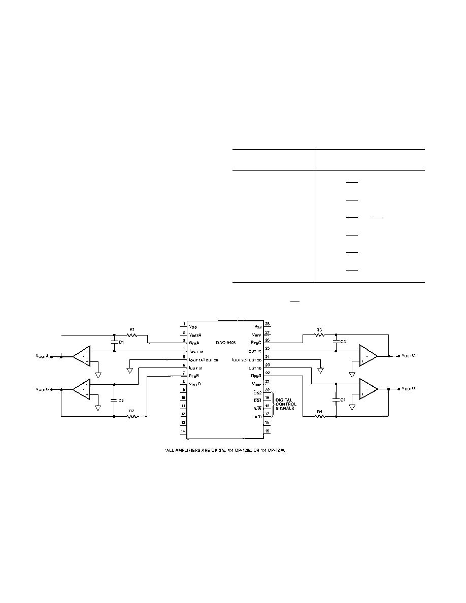
BASIC APPLICATIONS
Some basic circuit configurations are shown in Figures 6 and 7.
Figure 6 shows the DAC8408 connected in a unipolar configu-
ration (2-Quadrant Multiplication), and Table I shows the Code
Table. Resistors R1, R2, R3, and R4 are used to trim full scale
output. Full-scale output voltage = VREF –1 LSB = VREF (1–2
–8)
or VREF × (255/256) with all digital inputs high. Low tempera-
ture coefficient (approximately 50 ppm/
°C) resistors or trim-
mers should be selected if used. Full scale can also be adjusted
using VREF voltage. This will eliminate resistors R1, R2, R3, and
R4. In many applications, R1 through R4 are not required, and
the maximum gain error will then be that of the DAC.
Each DAC exhibits a variable output resistance that is code-
dependent. This produces a code-dependent, differential non-
linearity term at the amplifier’s output which can have a maxi-
mum value of 0.67
× the amplifier’s offset voltage. This differ-
ential nonlinearity term adds to the R-2R resistor ladder differ-
ential-nonlinearity; the output may no longer be monotonic. To
maintain monotonicity and minimize gain and linearity errors, it
is recommended that the op amp offset voltage be adjusted to
less than 10% of 1 LSB (1 LSB = 2
–8
× V
REF or 1/256
× V
REF),
or less than 3.9 mV over the operating temperature range. Zero-
scale output voltage (with all digital inputs low) may be adjusted
using the op amp offset adjustment. Capacitors C1, C2, C3,
and C4 provide phase compensation and help prevent overshoot
and ringing when using high speed op amps.
Figure 7 shows the recommended circuit configuration for the
bipolar operation (4-quadrant multiplication), and Table II shows
the Code Table. Trimmer resistors R17, R18, R19, and R20
are used only if gain error adjustments are required and range
between 50
and 1000 . Resistors R21, R22, R23, and R24
will range betwen 50
and 500 . If these resistors are used, it
is essential that resistor pairs R9–R13, R10–R14, R11–R15,
R12–R16 are matched both in value and tempco. They should
be within 0.01%; wire wound or metal foil types are preferred
for best temperature coefficient matching. The circuits of Figure
6 and 7 can either be used as a fixed reference D/A converter, or
as an attenuator with an ac input voltage.
Table I. Unipolar Binary Code Table (Refer to Figure 6)
DAC Data Input
MSB
LSB
Analog Output
1 1 1 1 1 1 1 1
–VREF
255
256
1 0 0 0 0 0 0 1
–VREF
129
256
1 0 0 0 0 0 0 0
–VREF
128
256
=
–VIN
2
0 1 1 1 1 1 1 1
–VREF
127
256
0 0 0 0 0 0 0 1
–VREF
1
256
0 0 0 0 0 0 0 0
–VREF
0
256
= 0
NOTE
1 LSB = (2
–8) (V
REF) =
1
256
(VREF)
Figure 6. Quad DAC Unipolar Operation (2-Quadrant Multiplication)
相关PDF资料 |
PDF描述 |
|---|---|
| VI-BTY-MX-F4 | CONVERTER MOD DC/DC 3.3V 49.5W |
| MS3126P12-10PZLC | CONN HSG PLUG 10POS STRGHT PINS |
| AD7398BRZ | IC DAC 12BIT QUAD SRL 16-SOIC |
| VI-BTY-MW-F4 | CONVERTER MOD DC/DC 3.3V 66W |
| DAC8562FSZ | IC DAC 12BIT PARALLEL 5V 20SOIC |
相关代理商/技术参数 |
参数描述 |
|---|---|
| DAC8408FSZ | 制造商:Analog Devices 功能描述:IC 8-BIT DAC |
| DAC8408FSZ-REEL | 功能描述:IC DAC 8BIT QUAD W/MEMORY 28SOIC RoHS:是 类别:集成电路 (IC) >> 数据采集 - 数模转换器 系列:- 标准包装:47 系列:- 设置时间:2µs 位数:14 数据接口:并联 转换器数目:1 电压电源:单电源 功率耗散(最大):55µW 工作温度:-40°C ~ 85°C 安装类型:表面贴装 封装/外壳:28-SSOP(0.209",5.30mm 宽) 供应商设备封装:28-SSOP 包装:管件 输出数目和类型:1 电流,单极;1 电流,双极 采样率(每秒):* |
| DAC8408FT | 制造商:Rochester Electronics LLC 功能描述:QUAD 8-BIT CMOS DAC WITH - Bulk |
| DAC8408G | 制造商:Analog Devices 功能描述: |
| DAC8408GBC | 制造商:未知厂家 制造商全称:未知厂家 功能描述:8-Bit Digital-to-Analog Converter |
发布紧急采购,3分钟左右您将得到回复。