参数资料
| 型号: | DAC8408GP |
| 厂商: | Analog Devices Inc |
| 文件页数: | 16/16页 |
| 文件大小: | 0K |
| 描述: | IC DAC 8BIT QUAD W/MEMORY 28-DIP |
| 产品培训模块: | Data Converter Fundamentals DAC Architectures |
| 标准包装: | 13 |
| 设置时间: | 190ns |
| 位数: | 8 |
| 数据接口: | 并联 |
| 转换器数目: | 4 |
| 电压电源: | 单电源 |
| 工作温度: | 0°C ~ 70°C |
| 安装类型: | 通孔 |
| 封装/外壳: | 28-DIP(0.600",15.24mm) |
| 供应商设备封装: | 28-PDIP |
| 包装: | 管件 |
| 输出数目和类型: | 4 电流,单极;4 电流,双极 |
| 采样率(每秒): | 5.26M |
DAC8408
–9–
REV. A
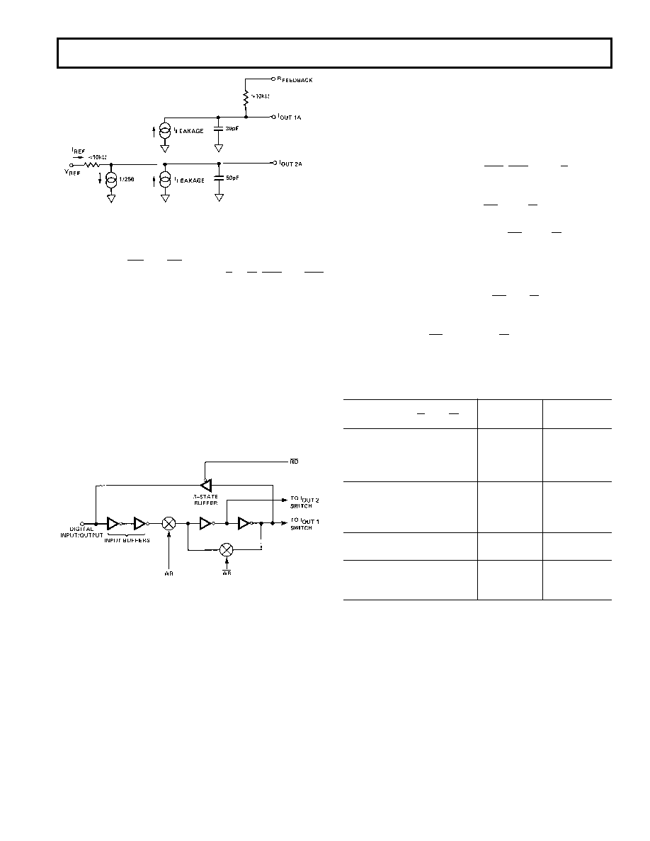
Figure 4. Equivalent DAC Circuit (AII Digital Inputs LOW)
DIGITAL SECTION
Figure 5 shows the digital input/output structure for one bit.
The digital WR, WR, and RD controls shown in the figure are
internally generated from the external A/B, R/W, DS1, and DS2
signals. The combination of these signals decide which DAC is
selected. The digital inputs are CMOS inverters, designed such
that TTL input levels (2.4 V and 0.8 V) are converted into
CMOS logic levels. When the digital input is in the region of 1.2 V
to 1.8 V, the input stages operate in their linear region and draw
current from the +5 V supply (see Typical Supply Current vs.
Logic Level curve on page 6). It is recommended that the digital
input voltages be as close to VDD and DGND as is practical in
order to minimize supply currents. This allows maximum sav-
ings in power dissipation inherent with CMOS devices. The
three-state readback digital output drivers (in the active mode)
provide TTL-compatible digital outputs with a fan-out of one
TTL load. The three state digital readback leakage-current is
typically 5 nA.
Figure 5. Digital Input/Output Structure
INTERFACE LOGIC SECTION
DAC Operating Modes
All DACs in HOLD MODE.
DAC A, B, C, or D individually selected (WRITE MODE).
DAC A, B, C, or D individually selected (READ MODE).
DACs A and C simultaneously selected (WRITE MODE).
DACs B and D simultaneously selected (WRITE MODE).
DAC Selection: Control inputs, DS1, DS2, and A/B select
which DAC can accept data from the input port (see Mode Se-
lection Table).
Mode Selection: Control inputs DS and R/W control the oper-
ating mode of the selected DAC.
Write Mode: When the control inputs DS and R/W are both
low, the selected DAC is in the write mode. The input data
latches of the selected DAC are transparent, and its analog out-
put responds to activity on the data inputs DB0–DB7.
Hold Mode: The selected DAC latch retains the data that was
present on the bus line just prior to DS or R/W going to a high
state. All analog outputs remain at the values corresponding to
the data in their respective latches.
Read Mode: When DS is low and R/W is high, the selected
DAC is in the read mode, and the data held in the appropriate
latch is put back onto the data bus.
MODE SELECTION TABLE
Control Logic
DS1
DS2
A/B
R/W
Mode
DAC
L
H
L
WRITE
A
L
H
L
WRITE
B
H
L
H
L
WRITE
C
H
L
WRITE
D
L
H
READ
A
L
H
L
H
READ
B
H
L
H
READ
C
H
L
H
READ
D
L
H
L
WRITE
A&C
L
WRITE
B&D
H
X
HOLD
A/B/C/D
L
H
HOLD
A/B/C/D
L
H
HOLD
A/B/C/D
L = Low State, H = High State, X = Irrelevant
相关PDF资料 |
PDF描述 |
|---|---|
| DAC8413EP | IC DAC 12BIT QUAD V-OUT 28-DIP |
| DAC8420FQ | IC DAC 12BIT QUAD SRL LP 16-CDIP |
| DAC8426EPZ | IC DAC 8BIT QUAD 10VREF 20PDIP |
| DAC8531IDRBTG4 | IC D/A CONV LP 16-BIT 8-SON |
| DAC8562FP | IC DAC 12BIT PARALLEL 5V 20-DIP |
相关代理商/技术参数 |
参数描述 |
|---|---|
| DAC8408GPZ | 功能描述:IC DAC 8BIT QUAD W/MEMORY 28DIP RoHS:是 类别:集成电路 (IC) >> 数据采集 - 数模转换器 系列:- 产品培训模块:Data Converter Fundamentals DAC Architectures 标准包装:750 系列:- 设置时间:7µs 位数:16 数据接口:并联 转换器数目:1 电压电源:双 ± 功率耗散(最大):100mW 工作温度:0°C ~ 70°C 安装类型:表面贴装 封装/外壳:28-LCC(J 形引线) 供应商设备封装:28-PLCC(11.51x11.51) 包装:带卷 (TR) 输出数目和类型:1 电压,单极;1 电压,双极 采样率(每秒):143k |
| DAC8408HP | 制造商:Rochester Electronics LLC 功能描述:- Bulk 制造商:Analog Devices 功能描述: |
| DAC8411 | 制造商:TI 制造商全称:Texas Instruments 功能描述:1.8V to 5.5V, 80mA, 14- and 16-Bit, Low-Power, Single-Channel,DIGITAL-TO-ANALOG CONVERTERS in SC70 Package |
| DAC8411EVM | 功能描述:数据转换 IC 开发工具 DAC8411 Eval Mod RoHS:否 制造商:Texas Instruments 产品:Demonstration Kits 类型:ADC 工具用于评估:ADS130E08 接口类型:SPI 工作电源电压:- 6 V to + 6 V |
| DAC8411EVM | 制造商:Texas Instruments 功能描述:Development Tool |
发布紧急采购,3分钟左右您将得到回复。