参数资料
| 型号: | DAC8413FPCZ |
| 厂商: | Analog Devices Inc |
| 文件页数: | 7/20页 |
| 文件大小: | 0K |
| 描述: | IC DAC 12BIT QUAD READBK 28-PLCC |
| 产品培训模块: | Data Converter Fundamentals DAC Architectures |
| 产品变化通告: | DAC8412/3 Redesign and Fab Process Change 01/Oct/2009 |
| 标准包装: | 1 |
| 设置时间: | 6µs |
| 位数: | 12 |
| 数据接口: | 并联 |
| 转换器数目: | 4 |
| 电压电源: | 单电源 |
| 功率耗散(最大): | 330mW |
| 工作温度: | -40°C ~ 85°C |
| 安装类型: | 表面贴装 |
| 封装/外壳: | 28-LCC(J 形引线) |
| 供应商设备封装: | 28-PLCC(11.51x11.51) |
| 包装: | 管件 |
| 输出数目和类型: | 4 电压,单极;4 电压,双极 |
| 采样率(每秒): | 167k |
Data Sheet
DAC8412/DAC8413
Rev. G | Page 15 of 20
RESET
The RESET function can be used either at power-up or at any
time during DAC operation. The RESET function is independent
of CS. This pin is active low and sets the DAC output registers
to either center code for the DAC8412, or zero code for the
DAC8413. The reset-to-center code is most useful when the
DAC is configured for bipolar references and an output of 0 V
after reset is desired.
SUPPLIES
Supplies required are VSS, VDD, and VLOGIC. The VSS supply can
be set between 15 V and 0 V. VDD is the positive supply; its
operating range is between 5 V and 15 V.
VLOGIC is the digital output supply voltage for the readback
function. It is normally connected to +5 V. This pin is a logic
reference input only. It does not supply current to the device. If
the readback function is not being used, VLOGIC can be left open-
circuit. While VLOGIC does not supply current to the DAC8412, it
does supply currents to the digital outputs when readback is used.
AMPLIFIERS
Unlike many voltage output DACs, the DAC8412 features buffered
voltage outputs. Each output is capable of both sourcing and
sinking 5 mA at ±10 V, eliminating the need for external
amplifiers when driving 500 pF or smaller capacitive load in
most applications. These amplifiers are short-circuit protected.
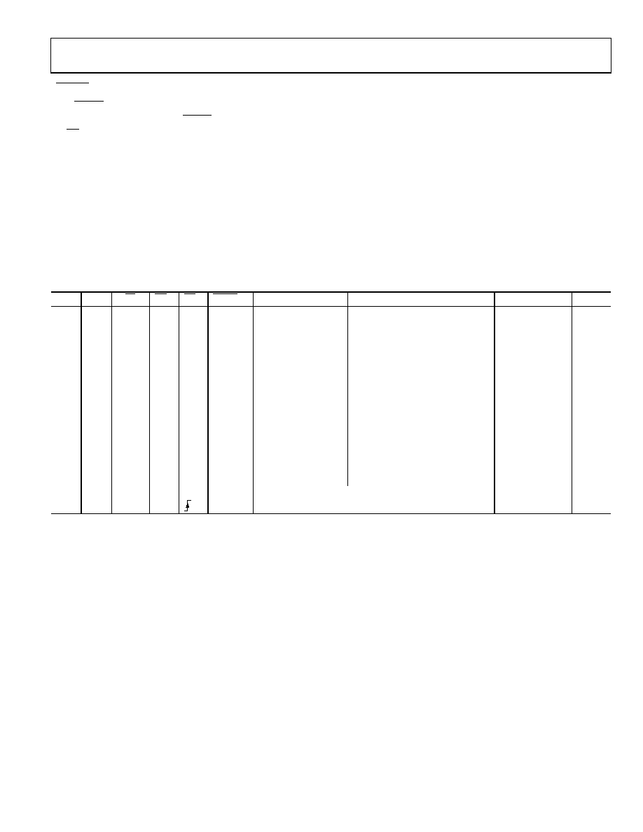
Table 6. DAC8412/DAC8413 Logic Table
A1
A0
R/W
CS
RS
LDAC
Input Register
Output Register
Mode
DAC
L
H
L
Write
Transparent
A
L
H
L
H
L
Write
Transparent
B
H
L
H
L
Write
Transparent
C
H
L
H
L
Write
Transparent
D
L
H
Write
Hold
Write input
A
L
H
L
H
Write
Hold
Write input
B
H
L
H
Write
Hold
Write input
C
H
L
H
Write
Hold
Write input
D
L
H
L
H
Read
Hold
Read input
A
L
H
L
H
Read
Hold
Read input
B
H
L
H
L
H
Read
Hold
Read input
C
H
L
H
Read
Hold
Read input
D
X
H
L
Hold
Update all output registers
All
X
H
Hold
All
X
L
X
All registers reset to midscale/zero-scale1
All
X
H
X
All registers latched to midscale/zero-scale1
All
1
DAC8412 resets to midscale, and DAC8413 resets to zero scale. L = logic low; H = logic high; X = don’t care. Input and output registers are transparent when asserted.
相关PDF资料 |
PDF描述 |
|---|---|
| VE-B64-MU-S | CONVERTER MOD DC/DC 48V 200W |
| VE-B60-MU-S | CONVERTER MOD DC/DC 5V 200W |
| VE-B5H-MU-S | CONVERTER MOD DC/DC 52V 200W |
| AD7228KPZ-REEL | IC DAC 8BIT OCTAL W/AMP 28-PLCC |
| VE-B5F-MU-S | CONVERTER MOD DC/DC 72V 200W |
相关代理商/技术参数 |
参数描述 |
|---|---|
| DAC8413FPCZ-REEL | 功能描述:IC DAC 12BIT QUAD V-OUT 28PLCC RoHS:是 类别:集成电路 (IC) >> 数据采集 - 数模转换器 系列:- 产品培训模块:Data Converter Fundamentals DAC Architectures 标准包装:750 系列:- 设置时间:7µs 位数:16 数据接口:并联 转换器数目:1 电压电源:双 ± 功率耗散(最大):100mW 工作温度:0°C ~ 70°C 安装类型:表面贴装 封装/外壳:28-LCC(J 形引线) 供应商设备封装:28-PLCC(11.51x11.51) 包装:带卷 (TR) 输出数目和类型:1 电压,单极;1 电压,双极 采样率(每秒):143k |
| DAC8413FPZ | 功能描述:IC DAC 12BIT QUAD V-OUT 28DIP RoHS:是 类别:集成电路 (IC) >> 数据采集 - 数模转换器 系列:- 标准包装:1 系列:- 设置时间:4.5µs 位数:12 数据接口:串行,SPI? 转换器数目:1 电压电源:单电源 功率耗散(最大):- 工作温度:-40°C ~ 125°C 安装类型:表面贴装 封装/外壳:8-SOIC(0.154",3.90mm 宽) 供应商设备封装:8-SOICN 包装:剪切带 (CT) 输出数目和类型:1 电压,单极;1 电压,双极 采样率(每秒):* 其它名称:MCP4921T-E/SNCTMCP4921T-E/SNRCTMCP4921T-E/SNRCT-ND |
| dac8413ft | 制造商:Rochester Electronics LLC 功能描述:- Bulk 制造商:Analog Devices 功能描述: |
| DAC8413FTC | 制造商:未知厂家 制造商全称:未知厂家 功能描述:12-Bit Digital-to-Analog Converter |
| DAC8420 | 制造商:AD 制造商全称:Analog Devices 功能描述:Quad 12-Bit Serial Voltage Output DAC |
发布紧急采购,3分钟左右您将得到回复。