参数资料
| 型号: | DAC8420ES |
| 厂商: | Analog Devices Inc |
| 文件页数: | 23/24页 |
| 文件大小: | 0K |
| 描述: | IC DAC 12BIT QUAD SRL-OUT 16SOIC |
| 产品培训模块: | Data Converter Fundamentals DAC Architectures |
| 标准包装: | 1 |
| 设置时间: | 8µs |
| 位数: | 12 |
| 数据接口: | 串行 |
| 转换器数目: | 4 |
| 电压电源: | 双 ± |
| 功率耗散(最大): | 255mW |
| 工作温度: | -40°C ~ 85°C |
| 安装类型: | 表面贴装 |
| 封装/外壳: | 16-SOIC(0.295",7.50mm 宽) |
| 供应商设备封装: | 16-SOIC W |
| 包装: | 管件 |
| 输出数目和类型: | 4 电压,单极;4 电压,双极 |
| 采样率(每秒): | 125k |
DAC8420
Rev. B | Page 8 of 24
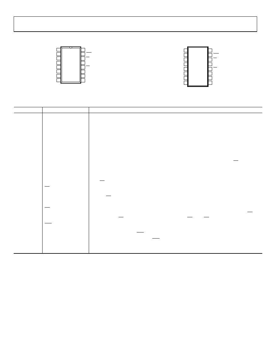
PIN CONFIGURATIONS AND FUNCTION DESCRIPTIONS
VDD 1
VOUTD 2
VOUTC 3
VREFLO 4
CLSEL
16
CLR
15
LD
14
NC
13
VREFHI 5
VOUTB 6
VOUTA 7
CS
12
CLK
11
SDI
10
VSS 8
GND
9
NC = NO CONNECT
DAC8420
TOP VIEW
(Not to Scale)
00
27
5-
0
04
Figure 4. PDIP and CERDIP
VDD 1
VOUTD 2
VOUTC 3
VREFLO 4
CLSEL
16
CLR
15
LD
14
NC
13
VREFHI 5
CS
12
VOUTB 6
CLK
11
VOUTA 7
SDI
10
VSS 8
GND
9
NC = NO CONNECT
DAC8420
TOP VIEW
(Not to Scale)
0
027
5-
00
5
Figure 5. SOIC
Table 5. Pin Function Descriptions
Pin No.
Mnemonic
Description
1
VDD
Positive Power Supply, 5 V to 15 V.
4
VREFLO
Reference Input. Lower DAC ladder reference voltage input, equal to zero-scale output. Allowable
range is VSS to (VVREFHI 2.5 V).
5
VREFHI
Reference Input. Upper DAC ladder reference voltage input. Allowable range is (VDD 2.5 V) to
(VVREFLO + 2.5 V).
7, 6, 3, 2
VOUTA through VOUTD
Buffered DAC Analog Voltage Outputs.
8
VSS
Negative Power Supply, 0 V to 15 V.
9
GND
Power Supply, Digital Ground.
10
SDI
Serial Data Input. Data presented to this pin is loaded into the internal serial-parallel shift register,
which shifts data in, beginning with DAC Address Bit A1. This input is ignored when CS is high. SDI
is CMOS/TTL compatible. The format of the 16-bit serial word is shown in Table 8.
11
CLK
System Serial Data Clock Input, TTL/CMOS Levels. Data presented to the input SDI is shifted into
the internal serial-parallel input register on the rising edge of clock. This input is logically OR’ed
with CS.
12
CS
Control Input, Device Chip Select, Active Low. This input is logically OR’ed with the clock and
disables the serial data register input when high. When low, data input clocking is enabled (see
Table 6). CS is CMOS/TTL compatible.
13
NC
No Connect = Don’t Care.
14
LD
Control Input, Asynchronous DAC Register Load Control, Active Low. The data currently contained
in the serial input shift register is shifted out to the DAC data registers on the falling edge of LD,
independent of CS. Input data must remain stable while LD is low. LD is CMOS/TTL compatible.
15
CLR
Control Input, Asynchronous Clear, Active Low. Sets internal data Register A through Register D to
zero or midscale, depending on current state of CLSEL. The data in the serial input shift register is
unaffected by this control. CLR is CMOS/TTL compatible.
16
CLSEL
Control Input, Determines action of CLR. If high, a clear command sets the internal DAC Register A
through Register D to midscale (0x800). If low, the registers are set to zero (0x000). CLSEL is CMOS
/
TTL compatible.
相关PDF资料 |
PDF描述 |
|---|---|
| VI-J2Z-MZ-B1 | CONVERTER MOD DC/DC 2V 10W |
| VE-JWK-MZ-B1 | CONVERTER MOD DC/DC 40V 25W |
| VE-JWH-MZ-B1 | CONVERTER MOD DC/DC 52V 25W |
| VE-B41-MU-S | CONVERTER MOD DC/DC 12V 200W |
| VE-JWF-MZ-B1 | CONVERTER MOD DC/DC 72V 25W |
相关代理商/技术参数 |
参数描述 |
|---|---|
| DAC8420ES-REEL | 功能描述:IC DAC 12BIT QUAD SRL LP 16-SOIC RoHS:否 类别:集成电路 (IC) >> 数据采集 - 数模转换器 系列:- 产品培训模块:Lead (SnPb) Finish for COTS Obsolescence Mitigation Program 标准包装:1,000 系列:- 设置时间:1µs 位数:8 数据接口:串行 转换器数目:8 电压电源:双 ± 功率耗散(最大):941mW 工作温度:0°C ~ 70°C 安装类型:表面贴装 封装/外壳:24-SOIC(0.295",7.50mm 宽) 供应商设备封装:24-SOIC W 包装:带卷 (TR) 输出数目和类型:8 电压,单极 采样率(每秒):* |
| DAC8420ESZ | 功能描述:IC DAC 12BIT QUAD SRL-OUT 16SOIC RoHS:是 类别:集成电路 (IC) >> 数据采集 - 数模转换器 系列:- 标准包装:1 系列:- 设置时间:4.5µs 位数:12 数据接口:串行,SPI? 转换器数目:1 电压电源:单电源 功率耗散(最大):- 工作温度:-40°C ~ 125°C 安装类型:表面贴装 封装/外壳:8-SOIC(0.154",3.90mm 宽) 供应商设备封装:8-SOICN 包装:剪切带 (CT) 输出数目和类型:1 电压,单极;1 电压,双极 采样率(每秒):* 其它名称:MCP4921T-E/SNCTMCP4921T-E/SNRCTMCP4921T-E/SNRCT-ND |
| DAC8420ESZ2 | 制造商:AD 制造商全称:Analog Devices 功能描述:Quad 12-Bit Serial Voltage Output DAC |
| DAC8420ESZ-REEL | 功能描述:IC DAC 12BIT QUAD SRL LP 16SOIC RoHS:是 类别:集成电路 (IC) >> 数据采集 - 数模转换器 系列:- 产品培训模块:Lead (SnPb) Finish for COTS Obsolescence Mitigation Program 标准包装:1,000 系列:- 设置时间:1µs 位数:8 数据接口:串行 转换器数目:8 电压电源:双 ± 功率耗散(最大):941mW 工作温度:0°C ~ 70°C 安装类型:表面贴装 封装/外壳:24-SOIC(0.295",7.50mm 宽) 供应商设备封装:24-SOIC W 包装:带卷 (TR) 输出数目和类型:8 电压,单极 采样率(每秒):* |
| DAC8420ESZ-REEL2 | 制造商:AD 制造商全称:Analog Devices 功能描述:Quad 12-Bit Serial Voltage Output DAC |
发布紧急采购,3分钟左右您将得到回复。