参数资料
| 型号: | DAC8512EPZ |
| 厂商: | Analog Devices Inc |
| 文件页数: | 1/20页 |
| 文件大小: | 0K |
| 描述: | IC DAC 12BIT SRL LP 5V 8DIP |
| 产品培训模块: | Data Converter Fundamentals DAC Architectures |
| 标准包装: | 1 |
| 设置时间: | 16µs |
| 位数: | 12 |
| 数据接口: | 串行 |
| 转换器数目: | 1 |
| 电压电源: | 单电源 |
| 功率耗散(最大): | 2.5mW |
| 工作温度: | -40°C ~ 85°C |
| 安装类型: | 通孔 |
| 封装/外壳: | 8-DIP(0.300",7.62mm) |
| 供应商设备封装: | 8-PDIP |
| 包装: | 管件 |
| 输出数目和类型: | 1 电压,单极;1 电压,双极 |
| 采样率(每秒): | 62.5k |
REV. A
Information furnished by Analog Devices is believed to be accurate and
reliable. However, no responsibility is assumed by Analog Devices for its
use, nor for any infringements of patents or other rights of third parties
which may result from its use. No license is granted by implication or
otherwise under any patent or patent rights of Analog Devices.
a
+5 V, Serial Input
Complete 12-Bit DAC
DAC8512
One Technology Way, P.O. Box 9106, Norwood, MA 02062-9106,
U.S.A.
Tel: 617/329-4700
World Wide Web Site: http://www.analog.com
Fax: 617/326-8703
Analog Devices, Inc., 1996
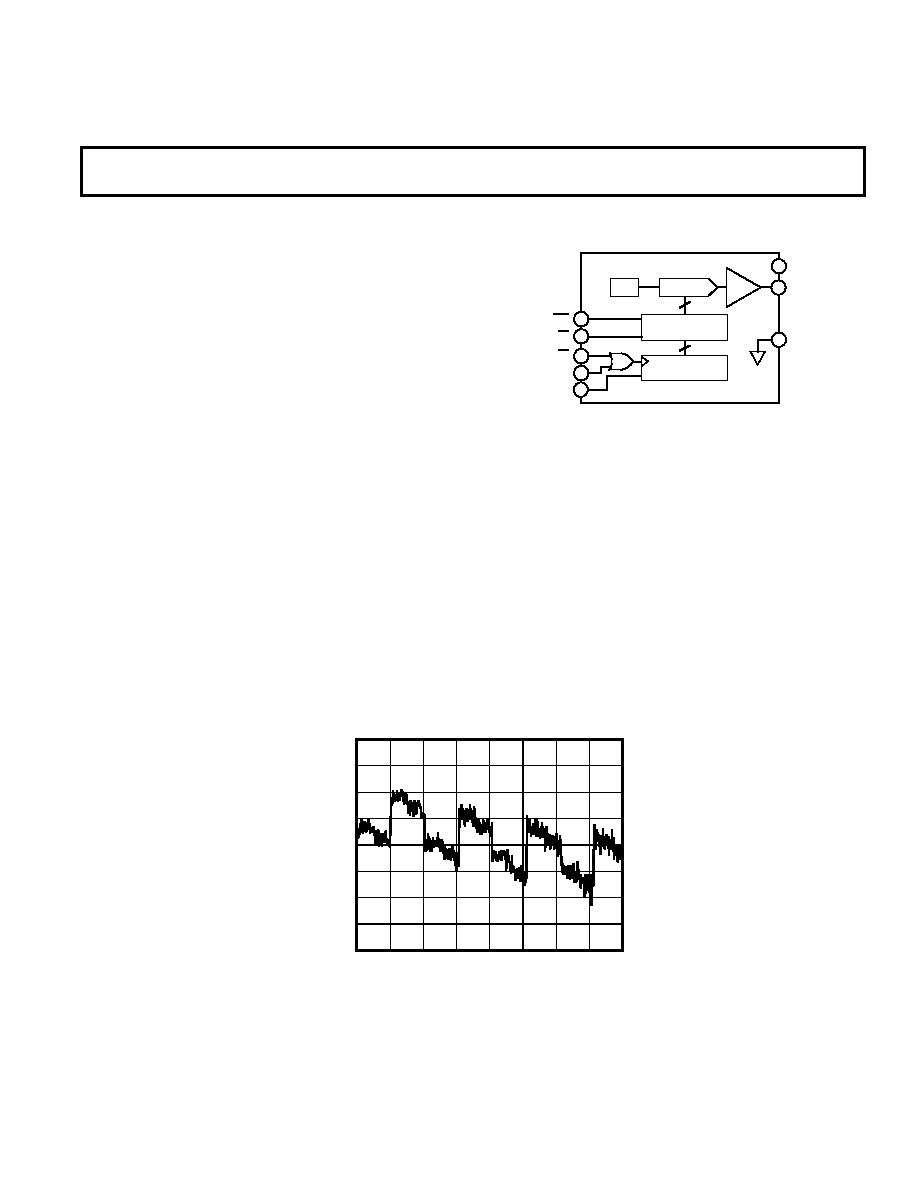
FUNCTIONAL BLOCK DIAGRAM
7
8
1
2
3
4
5
6
REF
12-BIT DAC
DAC REGISTER
VDD
VOUT
GND
SERIAL REGISTER
12
CLR
LD
CS
CLK
SDI
FEATURES
Space Saving SO-8 or Mini-DIP Packages
Complete, Voltage Output with Internal Reference
1 mV/Bit with 4.095 V Full Scale
Single +5 Volt Operation
No External Components
3-Wire Serial Data Interface, 20 MHz Data Loading Rate
Low Power: 2.5 mW
APPLICATIONS
Portable Instrumentation
Digitally Controlled Calibration
Servo Controls
Process Control Equipment
PC Peripherals
GENERAL DESCRIPTION
The DAC8512 is a complete serial input, 12-bit, voltage output
digital-to-analog converter designed to operate from a single
+5 V supply. It contains the DAC, input shift register and
latches, reference and a rail-to-rail output amplifier. Built using
a CBCMOS process, these monolithic DACs offer the user low
cost, and ease of use in +5 V only systems.
Coding for the DAC8512 is natural binary with the MSB loaded
first. The output op amp can swing to either rail and is set to a
range of 0 V to +4.095 V—for a one-millivolt-per-bit resolution.
It is capable of sinking and sourcing 5 mA. An on-chip reference
is laser trimmed to provide an accurate full-scale output voltage
of 4.095 V.
Serial interface is high speed, three-wire, DSP compatible with
data in (SDI), clock (CLK) and load strobe (LD). There is also
a chip-select pin for connecting multiple DACs.
A CLR input sets the output to zero scale at power on or upon
user demand.
The DAC8512 is specified over the extended industrial (–40
°C
to +85
°C) temperature range. DAC8512s are available in plas-
tic DIPs and SO-8 surface mount packages.
1.0
–1.0
4096
–0.5
–0.75
0
–0.25
0.25
0.5
0.75
3072
2048
1024
DIGITAL INPUT CODE – Decimal
LINEARITY
ERROR
–
LSB
Linearity Error vs. Digital Input Code
相关PDF资料 |
PDF描述 |
|---|---|
| AD7245JPZ | IC DAC 12BIT LC2MOS 28-PLCC |
| VI-B3Z-MX-B1 | CONVERTER MOD DC/DC 2V 30W |
| AD7245AAPZ | IC DAC 12BIT LC2MOS 28-PLCC |
| DAC8562FRU | IC DAC 12BIT PARALLEL 5V 20TSSOP |
| AD8522ANZ | IC DAC DUAL 12BIT 5V 14DIP |
相关代理商/技术参数 |
参数描述 |
|---|---|
| DAC8512EZ | 制造商:Rochester Electronics LLC 功能描述:- Bulk |
| DAC8512FP | 功能描述:IC DAC 12BIT 5V COMPLETE 8-DIP RoHS:否 类别:集成电路 (IC) >> 数据采集 - 数模转换器 系列:- 标准包装:2,400 系列:- 设置时间:- 位数:18 数据接口:串行 转换器数目:3 电压电源:模拟和数字 功率耗散(最大):- 工作温度:-40°C ~ 85°C 安装类型:表面贴装 封装/外壳:36-TFBGA 供应商设备封装:36-TFBGA 包装:带卷 (TR) 输出数目和类型:* 采样率(每秒):* |
| DAC8512FPZ | 功能描述:IC DAC 12BIT 5V COMPLETE 8-DIP RoHS:是 类别:集成电路 (IC) >> 数据采集 - 数模转换器 系列:- 产品培训模块:Lead (SnPb) Finish for COTS Obsolescence Mitigation Program 标准包装:50 系列:- 设置时间:4µs 位数:12 数据接口:串行 转换器数目:2 电压电源:单电源 功率耗散(最大):- 工作温度:-40°C ~ 85°C 安装类型:表面贴装 封装/外壳:8-TSSOP,8-MSOP(0.118",3.00mm 宽) 供应商设备封装:8-uMAX 包装:管件 输出数目和类型:2 电压,单极 采样率(每秒):* 产品目录页面:1398 (CN2011-ZH PDF) |
| DAC8512FS | 功能描述:IC DAC 12BIT 5V COMPLETE 8-SOIC RoHS:否 类别:集成电路 (IC) >> 数据采集 - 数模转换器 系列:- 标准包装:47 系列:- 设置时间:2µs 位数:14 数据接口:并联 转换器数目:1 电压电源:单电源 功率耗散(最大):55µW 工作温度:-40°C ~ 85°C 安装类型:表面贴装 封装/外壳:28-SSOP(0.209",5.30mm 宽) 供应商设备封装:28-SSOP 包装:管件 输出数目和类型:1 电流,单极;1 电流,双极 采样率(每秒):* |
| DAC8512FS-REEL | 制造商:Analog Devices 功能描述:DAC 1-CH R-2R 12-bit 8-Pin SOIC N T/R |
发布紧急采购,3分钟左右您将得到回复。