参数资料
| 型号: | DAC8512FS |
| 厂商: | Analog Devices Inc |
| 文件页数: | 17/20页 |
| 文件大小: | 0K |
| 描述: | IC DAC 12BIT 5V COMPLETE 8-SOIC |
| 产品培训模块: | Data Converter Fundamentals DAC Architectures |
| 标准包装: | 1 |
| 设置时间: | 16µs |
| 位数: | 12 |
| 数据接口: | 串行 |
| 转换器数目: | 1 |
| 电压电源: | 单电源 |
| 功率耗散(最大): | 2.5mW |
| 工作温度: | -40°C ~ 85°C |
| 安装类型: | 表面贴装 |
| 封装/外壳: | 8-SOIC(0.154",3.90mm 宽) |
| 供应商设备封装: | 8-SOIC |
| 包装: | 管件 |
| 输出数目和类型: | 1 电压,单极;1 电压,双极 |
| 采样率(每秒): | 62.5k |
DAC8512
–6–
REV. A
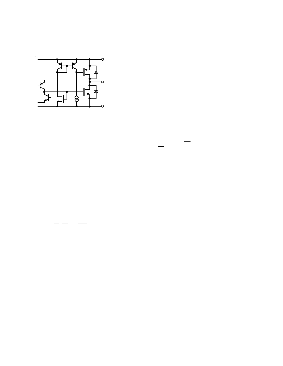
OUTPUT SECTION
The rail-to-rail output stage of this amplifier has been designed
to provide precision performance while operating near either
power supply.
VDD
VOUT
AGND
N-CH
P-CH
Figure 4. Equivalent Analog Output Circuit
Figure 4 shows an equivalent output schematic of the rail-to-rail
amplifier with its N channel pull down FETs that will pull an
output load directly to GND. The output sourcing current is
provided by a P channel pull up device that can supply GND
terminated loads, especially at the low supply tolerance values of
4.75 volts. Figures 5 and 6 provide information on output swing
performance near ground and full-scale as a function of load. In
addition to resistive load driving capability the amplifier has also
been carefully designed and characterized for up to 500 pF ca-
pacitive load driving capability.
POWER SUPPLY
The very low power consumption of the DAC8512 is a direct
result of a circuit design optimizing use of the CBCMOS pro-
cess. By using the low power characteristics of the CMOS for
the logic, and the low noise, tight matching of the complemen-
tary bipolar transistors good analog accuracy is achieved.
For power consumption sensitive applications it is important to
note that the internal power consumption of the DAC8512 is
strongly dependent on the actual logic input voltage levels
present on the SDI, CS, LD, and CLR pins. Since these inputs
are standard CMOS logic structures they contribute static
power dissipation dependent on the actual driving logic VOH and
VOL voltage levels. The graph in Figure 9 shows the effect on to-
tal DAC8512 supply current as a function of the actual value of
input logic voltage. Consequently use of CMOS logic vs. TTL
minimizes power dissipation in the static state. A VIL = 0 V on
the SDI, CS and CLR pins provides the lowest standby power
dissipation of 2.5 mW (500
A × 5 V).
As with any analog system, it is recommended that the DAC8512
power supply be bypassed on the same PC card that contains the
chip. Figure 10 shows the power supply rejection versus frequen-
cy performance. This should be taken into account when using
higher frequency switched mode power supplies with ripple fre-
quencies of 100 kHz and higher.
One advantage of the rail-to-rail output amplifier used in the
DAC8512 is the wide range of usable supply voltage. The part
is fully specified and tested over temperature for operation from
+4.75 V to +5.25 V. If reduced linearity and source current ca-
pability near full scale can be tolerated, operation of the DAC8512
is possible down to +4.3 volts. The minimum operating supply
voltage versus load current plot, in Figure 11, provides informa-
tion for operation below VDD = +4.75 V.
TIMING AND CONTROL
The DAC8512 has a separate serial input register from the
12-bit DAC register that allows preloading of a new data value
into the serial register without disturbing the present DAC out-
put voltage. After the new value is fully loaded in the serial in-
put register it can be asynchronously transferred to the DAC
register by strobing the LD pin. The DAC register uses a level
sensitive LD strobe that should be returned high before any
new data is loaded into the serial input register. At any time the
contents of the DAC register can be reset to zero by strobing
the CLR pin which causes the DAC output voltage to go to
zero volts. All of the timing requirements are detailed in Figure
1 along with the Table I Control-Logic Truth Table.
相关PDF资料 |
PDF描述 |
|---|---|
| VI-213-IV-F1 | CONVERTER MOD DC/DC 24V 150W |
| AD1953YSTZRL7 | IC DSP AUDIO 3CHAN 26BIT 48LQFP |
| LTC1657CGN#TR | IC DAC 16BIT R-R MICROPWR 28SSOP |
| VI-25F-MW-B1 | CONVERTER MOD DC/DC 72V 100W |
| VI-21P-IV-F4 | CONVERTER MOD DC/DC 13.8V 150W |
相关代理商/技术参数 |
参数描述 |
|---|---|
| DAC8512FS-REEL | 制造商:Analog Devices 功能描述:DAC 1-CH R-2R 12-bit 8-Pin SOIC N T/R |
| DAC8512FS-REEL7 | 功能描述:IC DAC 12BIT SRL LP 5V 8-SOIC RoHS:否 类别:集成电路 (IC) >> 数据采集 - 数模转换器 系列:- 标准包装:47 系列:- 设置时间:2µs 位数:14 数据接口:并联 转换器数目:1 电压电源:单电源 功率耗散(最大):55µW 工作温度:-40°C ~ 85°C 安装类型:表面贴装 封装/外壳:28-SSOP(0.209",5.30mm 宽) 供应商设备封装:28-SSOP 包装:管件 输出数目和类型:1 电流,单极;1 电流,双极 采样率(每秒):* |
| DAC8512FSZ | 功能描述:IC DAC 12BIT 5V COMPLETE 8-SOIC RoHS:是 类别:集成电路 (IC) >> 数据采集 - 数模转换器 系列:- 产品培训模块:Lead (SnPb) Finish for COTS Obsolescence Mitigation Program 标准包装:50 系列:- 设置时间:4µs 位数:12 数据接口:串行 转换器数目:2 电压电源:单电源 功率耗散(最大):- 工作温度:-40°C ~ 85°C 安装类型:表面贴装 封装/外壳:8-TSSOP,8-MSOP(0.118",3.00mm 宽) 供应商设备封装:8-uMAX 包装:管件 输出数目和类型:2 电压,单极 采样率(每秒):* 产品目录页面:1398 (CN2011-ZH PDF) |
| DAC8512FSZ-REEL | 功能描述:IC DAC 12BIT SRL LP 5V 8SOIC RoHS:是 类别:集成电路 (IC) >> 数据采集 - 数模转换器 系列:- 产品培训模块:LTC263x 12-, 10-, and 8-Bit VOUT DAC Family 特色产品:LTC2636 - Octal 12-/10-/8-Bit SPI VOUT DACs with 10ppm/°C Reference 标准包装:91 系列:- 设置时间:4µs 位数:10 数据接口:MICROWIRE?,串行,SPI? 转换器数目:8 电压电源:单电源 功率耗散(最大):2.7mW 工作温度:-40°C ~ 85°C 安装类型:表面贴装 封装/外壳:14-WFDFN 裸露焊盘 供应商设备封装:14-DFN-EP(4x3) 包装:管件 输出数目和类型:8 电压,单极 采样率(每秒):* |
| DAC8512FSZ-REEL7 | 功能描述:IC DAC 12BIT SRL LP 5V 8SOIC RoHS:是 类别:集成电路 (IC) >> 数据采集 - 数模转换器 系列:- 产品培训模块:LTC263x 12-, 10-, and 8-Bit VOUT DAC Family 特色产品:LTC2636 - Octal 12-/10-/8-Bit SPI VOUT DACs with 10ppm/°C Reference 标准包装:91 系列:- 设置时间:4µs 位数:10 数据接口:MICROWIRE?,串行,SPI? 转换器数目:8 电压电源:单电源 功率耗散(最大):2.7mW 工作温度:-40°C ~ 85°C 安装类型:表面贴装 封装/外壳:14-WFDFN 裸露焊盘 供应商设备封装:14-DFN-EP(4x3) 包装:管件 输出数目和类型:8 电压,单极 采样率(每秒):* |
发布紧急采购,3分钟左右您将得到回复。