- 您现在的位置:买卖IC网 > PDF目录17091 > DAC8531EVM (Texas Instruments)EVAL MOD FOR DAC8531 PDF资料下载
参数资料
| 型号: | DAC8531EVM |
| 厂商: | Texas Instruments |
| 文件页数: | 6/27页 |
| 文件大小: | 0K |
| 描述: | EVAL MOD FOR DAC8531 |
| 产品培训模块: | Data Converter Basics |
| 标准包装: | 1 |
| DAC 的数量: | 1 |
| 位数: | 16 |
| 数据接口: | SPI?、QSPI?、MICROWIRE? 和 DSP |
| 设置时间: | 8µs |
| DAC 型: | 电压 |
| 工作温度: | -40°C ~ 105°C |
| 已供物品: | 板 |
| 已用 IC / 零件: | DAC8531 |
| 产品目录页面: | 900 (CN2011-ZH PDF) |
| 相关产品: | DAC8531E/250DKR-ND - IC D/A CONV LP 16-BIT 8-MSOP DAC8531IDRBTG4-ND - IC D/A CONV LP 16-BIT 8-SON DAC8531IDRBRG4-ND - IC D/A CONV LP 16-BIT 8-SON DAC8531IDRBR-ND - IC D/A CONV LP 16-BIT 8-SON DAC8531E/2K5G4-ND - IC D/A CONV LP 16-BIT 8-MSOP DAC8531E/2K5-ND - IC D/A CONV LP 16-BIT 8-MSOP DAC8531E/250G4-ND - IC D/A CONV LP 16-BIT 8-MSOP 296-15727-6-ND - IC DAC 16BIT RRO LP 8-SON 296-15727-2-ND - IC DAC 16BIT RRO LP 8-SON 296-15727-1-ND - IC DAC 16BIT RRO LP 8-SON 更多... |
| 其它名称: | 296-13548 |
第1页第2页第3页第4页第5页当前第6页第7页第8页第9页第10页第11页第12页第13页第14页第15页第16页第17页第18页第19页第20页第21页第22页第23页第24页第25页第26页第27页
DAC8531
14
SBAS192B
www.ti.com
power supply is quite noisy or if the system supply voltages
are at some value other than 5V. The REF02 will output a
steady supply voltage for the DAC8531. If the REF02 is
used, the typical current it needs to supply to the DAC8531
is 250
A. This is with no load on the output of the DAC.
When the DAC output is loaded, the REF02 also needs to
supply the current to the load. The total current required (with
a 5k
load on the DAC output) is:
250
A + (5V/5k) = 1.29mA
The load regulation of the REF02 is typically 0.005%/mA,
which results in an error of 322
V for the 1.29mA current
drawn from it. This corresponds to a 4.2LSB error.
BIPOLAR OPERATION USING THE DAC8531
The DAC8531 has been designed for single-supply operation
but a bipolar output range is also possible using the circuit in
Figure 10. The circuit shown will give an output voltage range
of
±V
REF. Rail-to-rail operation at the amplifier output is achiev-
able using an OPA703 as the output amplifier.
The output voltage for any input code can be calculated as
follows:
VV
D
RR
R
V
R
O
REF
=
+
65536
12
1
2
1
–
where D represents the input code in decimal (0–65535).
With VREF = 5V, R1 = R2 = 10k:
V
D
V
O =
10
65536
5
–
This is an output voltage range of
±5V with 0000
H corre-
sponding to a –5V output and FFFFH corresponding to a +5V
output. Similarly, using VREF = 2.5V, ±2.5V output voltage
raw can be achieved.
LAYOUT
A precision analog component requires careful layout, ad-
equate bypassing, and clean, well-regulated power supplies.
As the DAC8531 offers single-supply operation, it will often
be used in close proximity with digital logic, microcontrollers,
microprocessors, and digital signal processors. The more
digital logic present in the design and the higher the switch-
ing speed, the more difficult it will be to keep digital noise
from appearing at the output.
Due to the single ground pin of the DAC8531, all return
currents, including digital and analog return currents, must
flow through the GND pin. Ideally, GND would be connected
directly to an analog ground plane. This plane would be
separate from the ground connection for the digital compo-
nents until they were connected at the power-entry point of
the system.
The 68HC11 should be configured so that its CPOL bit is a
0 and its CPHA bit is a 1. This configuration causes data
appearing on the MOSI output to be valid on the falling edge
of SCK. When data is being transmitted to the DAC, the
SYNC line is taken LOW (PC7). Serial data from the 68HC11
is transmitted in 8-bit bytes with only eight falling clock edges
occurring in the transmit cycle. Data is transmitted MSB first.
In order to load data to the DAC8531, PC7 is left LOW after
the first eight bits are transferred, then a second and third
serial write operation is performed to the DAC and PC7 is
taken HIGH at the end of this procedure.
APPLICATIONS
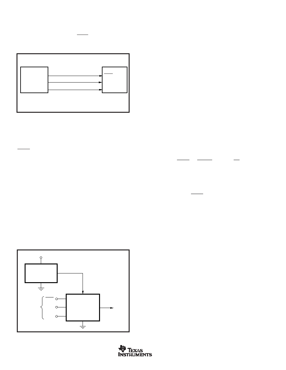
USING REF02 AS A POWER SUPPLY FOR
THE DAC8531
Due to the extremely low supply current required by the
DAC8531, an alternative option is to use a REF02 +5V
precision voltage reference to supply the required voltage to
the part, as shown in Figure 9. This is especially useful if the
FIGURE 8. DAC8531 to 68HC11 Interface.
FIGURE 9. REF02 as a Power Supply to the DAC8531.
DAC8531 TO 68HC11 INTERFACE
Figure 8 shows a serial interface between the DAC8531 and
the 68HC11 microcontroller. SCK of the 68HC11 drives the
SCLK of the DAC8531, while the MOSI output drives the
serial data line of the DAC. The SYNC signal is derived from
a port line (PC7), similar to what was done for the 8051.
68HC11(1)
PC7
SCK
MOSI
SYNC
SCLK
D
IN
DAC8531(1)
NOTE: (1) Additional pins omitted for clarity.
REF02
DAC8531
Three-Wire
Serial
Interface
+5V
285
A
V
OUT = 0V to 5V
SYNC
SCLK
D
IN
+15
相关PDF资料 |
PDF描述 |
|---|---|
| AP2101MPG-13 | IC USB SWITCH 2.45A CURR 8MSOP |
| EMM06DRYI-S13 | CONN EDGECARD 12POS .156 EXTEND |
| ADS8364M-EVM | EVAL MODULE FOR ADS8364 |
| AP2111SG-13 | IC USB SWITCH 2.45A CURRENT 8SOP |
| SDR-V | SCOTCH CODE REFILL V |
相关代理商/技术参数 |
参数描述 |
|---|---|
| DAC8531IDRB | 制造商:Texas Instruments 功能描述: |
| DAC8531IDRBR | 功能描述:数模转换器- DAC Lo-Pwr R-to-R Out 16-Bit Serial Input RoHS:否 制造商:Texas Instruments 转换器数量:1 DAC 输出端数量:1 转换速率:2 MSPs 分辨率:16 bit 接口类型:QSPI, SPI, Serial (3-Wire, Microwire) 稳定时间:1 us 最大工作温度:+ 85 C 安装风格:SMD/SMT 封装 / 箱体:SOIC-14 封装:Tube |
| DAC8531IDRBRG4 | 功能描述:数模转换器- DAC Lo-Pwr R-to-R Out 16-Bit Serial Input RoHS:否 制造商:Texas Instruments 转换器数量:1 DAC 输出端数量:1 转换速率:2 MSPs 分辨率:16 bit 接口类型:QSPI, SPI, Serial (3-Wire, Microwire) 稳定时间:1 us 最大工作温度:+ 85 C 安装风格:SMD/SMT 封装 / 箱体:SOIC-14 封装:Tube |
| DAC8531IDRBT | 功能描述:数模转换器- DAC Lo-Pwr R-to-R Out 16-Bit Serial Input RoHS:否 制造商:Texas Instruments 转换器数量:1 DAC 输出端数量:1 转换速率:2 MSPs 分辨率:16 bit 接口类型:QSPI, SPI, Serial (3-Wire, Microwire) 稳定时间:1 us 最大工作温度:+ 85 C 安装风格:SMD/SMT 封装 / 箱体:SOIC-14 封装:Tube |
| DAC8531IDRBTG4 | 功能描述:数模转换器- DAC Lo-Pwr R-to-R Out 16-Bit Serial Input RoHS:否 制造商:Texas Instruments 转换器数量:1 DAC 输出端数量:1 转换速率:2 MSPs 分辨率:16 bit 接口类型:QSPI, SPI, Serial (3-Wire, Microwire) 稳定时间:1 us 最大工作温度:+ 85 C 安装风格:SMD/SMT 封装 / 箱体:SOIC-14 封装:Tube |
发布紧急采购,3分钟左右您将得到回复。