- 您现在的位置:买卖IC网 > PDF目录170654 > DAC8551IADGKTG4 (TEXAS INSTRUMENTS INC) SERIAL INPUT LOADING, 12 us SETTLING TIME, 16-BIT DAC, PDSO8 PDF资料下载
参数资料
| 型号: | DAC8551IADGKTG4 |
| 厂商: | TEXAS INSTRUMENTS INC |
| 元件分类: | DAC |
| 英文描述: | SERIAL INPUT LOADING, 12 us SETTLING TIME, 16-BIT DAC, PDSO8 |
| 封装: | GREEN, PLASTIC, MSOP-8 |
| 文件页数: | 8/24页 |
| 文件大小: | 456K |
| 代理商: | DAC8551IADGKTG4 |
www.ti.com
SYNC INTERRUPT
INPUT SHIFT REGISTER
POWER-ON RESET
CLK
SYNC
D
IN
ValidWriteSequence:OutputUpdates
onthe24thFallingEdge
24thFallingEdge
DB23
DB80
DB23
DB80
SLAS429B – APRIL 2005 – REVISED OCTOBER 2006
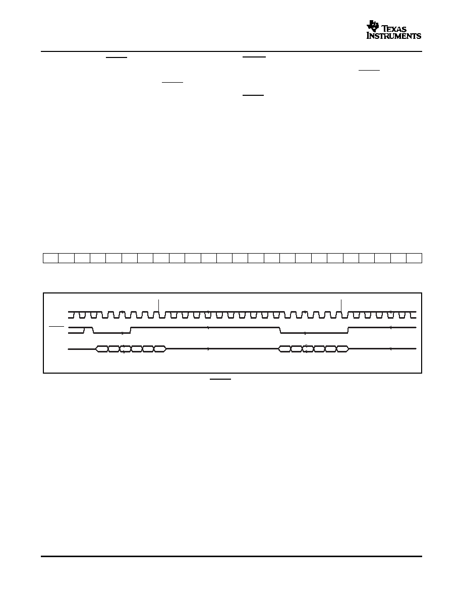
At this point, the SYNC line may be kept LOW or
brought HIGH. In either case, it must be brought
In a normal write sequence, the SYNC line is kept
HIGH for a minimum of 33ns before the next write
LOW for at least 24 falling edges of SCLK and the
sequence so that a falling edge of SYNC can initiate
DAC is updated on the 24th falling edge. However, if
the next write sequence. As previously mentioned, it
SYNC is brought HIGH before the 24th falling edge,
must be brought HIGH again just before the next
it acts as an interrupt to the write sequence. The shift
write sequence.
register is reset, and the write sequence is seen as
invalid. Neither an update of the DAC register
contents nor a change in the operating mode occurs,
as shown in Figure 48.
The input shift register is 24 bits wide, as shown in
Figure 47. The first six bits are don't care bits. The
next two bits (PD1 andPD0) are control bits that
control which mode of operation the part is in
The DAC8551 contains a power-on-reset circuit that
(normal mode or any one of three power-down
controls the output voltage during power up. On
modes). A more complete description of the various
power up, the DAC registers are filled with zeros and
modes is located in the Power-Down Modes section.
the output voltages are 0V; they remain that way
The next 16 bits are the data bits. These bits are
until a valid write sequence is made to the DAC. The
transferred to the DAC register on the 24th falling
power-on reset is useful in applications where it is
edge of SCLK.
important to know the state of the output of the DAC
while it is in the process of powering up.
DB23
DB0
X
PD1
PD0
D15
D14
D13
D12
D11
D10
D9
D8
D7
D6
D5
D4
D3
D2
D1
D0
Figure 47. DAC8551 Data Input Register Format
Figure 48. SYNC Interrupt Facility
16
相关PDF资料 |
PDF描述 |
|---|---|
| DAC8551IADGKT | SERIAL INPUT LOADING, 12 us SETTLING TIME, 16-BIT DAC, PDSO8 |
| DAC8551IADGKRG4 | SERIAL INPUT LOADING, 12 us SETTLING TIME, 16-BIT DAC, PDSO8 |
| DAC8554IPWR | SERIAL INPUT LOADING, 12 us SETTLING TIME, 16-BIT DAC, PDSO16 |
| DAC8554IPW | SERIAL INPUT LOADING, 12 us SETTLING TIME, 16-BIT DAC, PDSO16 |
| DAC8564IAPWR | SERIAL INPUT LOADING, 12 us SETTLING TIME, 16-BIT DAC, PDSO16 |
相关代理商/技术参数 |
参数描述 |
|---|---|
| DAC8551IDGK | 功能描述:数模转换器- DAC 16-Bit UltrLo Glitch Vltg Output RoHS:否 制造商:Texas Instruments 转换器数量:1 DAC 输出端数量:1 转换速率:2 MSPs 分辨率:16 bit 接口类型:QSPI, SPI, Serial (3-Wire, Microwire) 稳定时间:1 us 最大工作温度:+ 85 C 安装风格:SMD/SMT 封装 / 箱体:SOIC-14 封装:Tube |
| DAC8551IDGKR | 功能描述:数模转换器- DAC 16-Bit UltrLo Glitch Vltg Output RoHS:否 制造商:Texas Instruments 转换器数量:1 DAC 输出端数量:1 转换速率:2 MSPs 分辨率:16 bit 接口类型:QSPI, SPI, Serial (3-Wire, Microwire) 稳定时间:1 us 最大工作温度:+ 85 C 安装风格:SMD/SMT 封装 / 箱体:SOIC-14 封装:Tube |
| DAC8551IDGKRG4 | 功能描述:数模转换器- DAC 16-Bit UltrLo Glitch Vltg Output RoHS:否 制造商:Texas Instruments 转换器数量:1 DAC 输出端数量:1 转换速率:2 MSPs 分辨率:16 bit 接口类型:QSPI, SPI, Serial (3-Wire, Microwire) 稳定时间:1 us 最大工作温度:+ 85 C 安装风格:SMD/SMT 封装 / 箱体:SOIC-14 封装:Tube |
| DAC8551IDGKT | 功能描述:数模转换器- DAC 16-Bit UltrLo Glitch Vltg Output RoHS:否 制造商:Texas Instruments 转换器数量:1 DAC 输出端数量:1 转换速率:2 MSPs 分辨率:16 bit 接口类型:QSPI, SPI, Serial (3-Wire, Microwire) 稳定时间:1 us 最大工作温度:+ 85 C 安装风格:SMD/SMT 封装 / 箱体:SOIC-14 封装:Tube |
| DAC8551IDGKT | 制造商:Texas Instruments 功能描述:D/A CONVERTER (D-A) IC ((NW)) 制造商:Texas Instruments 功能描述:IC, DAC, 16BIT, 200KSPS, MSOP-8 |
发布紧急采购,3分钟左右您将得到回复。