参数资料
| 型号: | DAC8562FP |
| 厂商: | Analog Devices Inc |
| 文件页数: | 4/16页 |
| 文件大小: | 0K |
| 描述: | IC DAC 12BIT PARALLEL 5V 20-DIP |
| 产品培训模块: | Data Converter Fundamentals DAC Architectures |
| 标准包装: | 18 |
| 设置时间: | 16µs |
| 位数: | 12 |
| 数据接口: | 并联 |
| 转换器数目: | 1 |
| 电压电源: | 单电源 |
| 功率耗散(最大): | 30mW |
| 工作温度: | -40°C ~ 85°C |
| 安装类型: | 通孔 |
| 封装/外壳: | 20-DIP(0.300",7.62mm) |
| 供应商设备封装: | 20-PDIP |
| 包装: | 管件 |
| 输出数目和类型: | 1 电压,单极;1 电压,双极 |
| 采样率(每秒): | 62.5k |
DAC8562
REV. A
–12–
Alternatively, the output voltage can be coded in complementary
offset binary using the circuit in Figure 35. This configuration
eliminates the need for a pull-down resistor or an op amp for
REFOUT The transfer equation of the circuit is given by:
V
O = –1 mV × Digital Code ×
R2
R1
+ REFOUT
×
R4
R3
+ R4
× 1+
R2
R1
and, for the values shown, becomes:
V
O =2. 44 mV × Digital Code + 5 V
DAC-8562
REFOUT
VOUT
R1
R4
R3
R2
VO
RANGE
±5V
R2
23.7k + 715
R4
13.7k + 169
R1 = R3 = 10k
Figure 35 Bipolar Output Operation Without
Trim Version 2
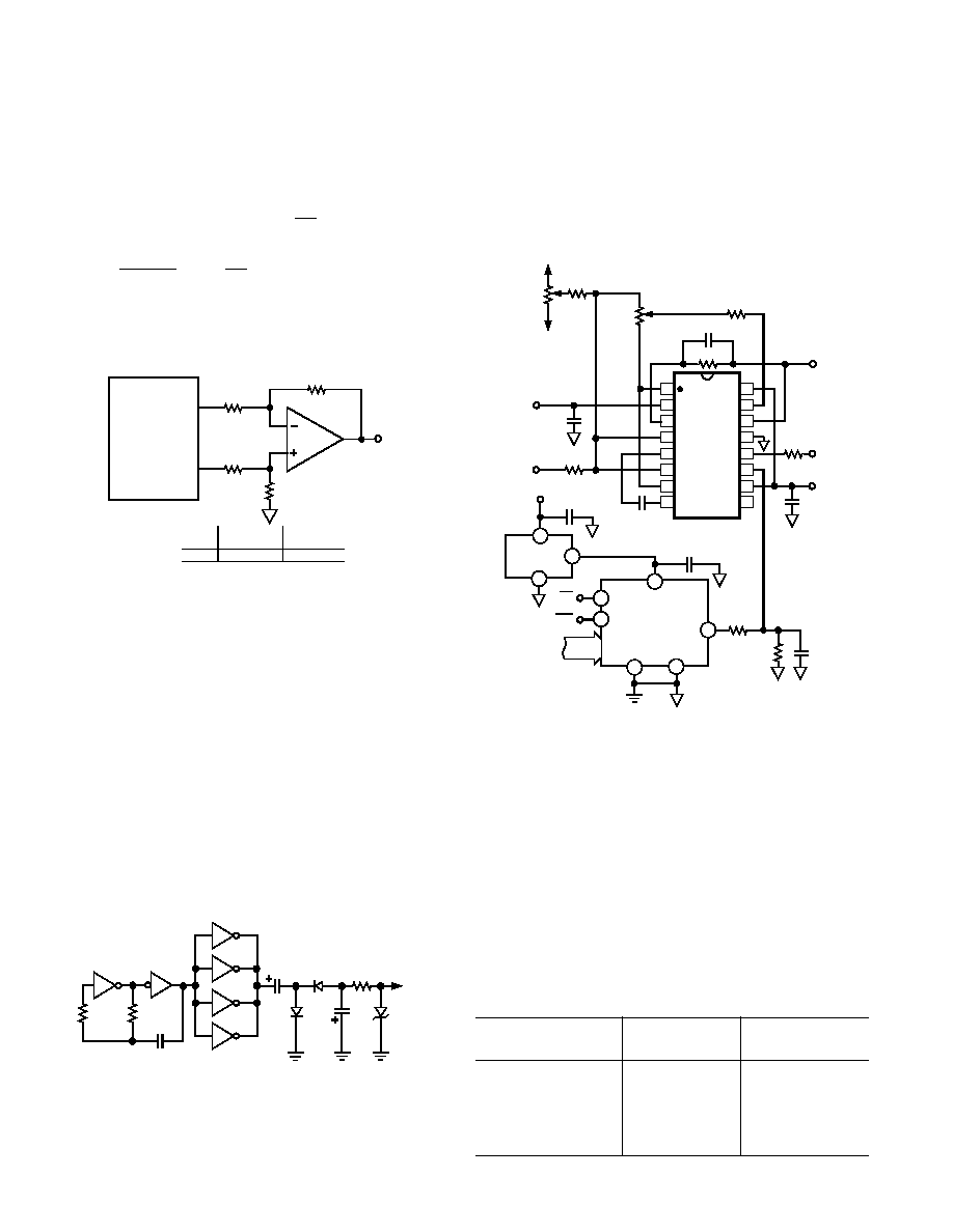
Generating a Negative Supply Voltage
Some applications may require bipolar output configuration, but
only have a single power supply rail available. This is very com-
mon in data acquisition systems using microprocessor-based sys-
tems. In these systems, only +12 V, +15 V, and/or +5 V are
available. Shown in Figure 36 is a method of generating a nega-
tive supply voltage using one CD4049, a CMOS hex inverter,
operating on +12 V or +15 V. The circuit is essentially a charge
pump where two of the six are used as an oscillator. For the val-
ues shown, the frequency of oscillation is approximately 3.5 kHz
and is fairly insensitive to supply voltage because R1 > 2
R2.
The remaining four inverters are wired in parallel for higher out-
put current. The square-wave output is level translated by C2 to
a negative-going signal, rectified using a pair of 1N4001s, and
then filtered by C3. With the values shown, the charge pump
will provide an output voltage of –5 V for current loading in the
range 0.5 mA
≤ I
OUT
≤ 10 mA with a +15 V supply and
0.5 mA
≤ I
OUT
≤ 7 mA with a +12 V supply.
910
6
11
12
14
15
7
32
5
4
R2
5.1k
R1
510k
C1
0.02F
C2
47F
D1
1N4001
C3
47F
1N5231
5.1V
ZENER
D2
1N4001
R3
470
–5V
INVERTERS = CD4049
Figure 36. Generating a –5 V Supply When
Only +12 V or +15 V Are Available
Audio Volume Control
The DAC8562 is well suited to control digitally the gain or
attenuation of a voltage controlled amplifiers. In professional
audio mixing consoles, music synthesizers, and other audio proces-
sors, VCAs, such as the SSM2018, adjust audio channel gain and
attenuation from front panel potentiometers. The VCA provides a
clean gain transition control of the audio level when the slew rate of
the analog input control voltage, VC, is properly chosen. The cir-
cuit in Figure 37 illustrates a volume control application using the
DAC8562 to control the attenuation of the SSM2018.
15
16
DGND
AGND
DATA
DAC-8562
13
+15V
10
CE
CLR
20
12
0.1F
4
REF-02
6
2
0.1F
18k
10pF
470k
P1
100k
10M
OFFSET
TRIM
47pF
SYMMETRY
TRIM
P2
500k
VOUT
+15V
–15V
30k
+15V
–15V
0.1F
+15V
18k
VIN
1
2
3
4
5
6
7
8
16
15
14
13
12
11
10
9
SSM-2018
+5V
CCON
1F
R6
825
R7
1k
*
0V
≤ V
C ≤ +2.24V
* – PRECISION RESISTOR PT146
1k
COMPENSATOR
Figure 37. Audio Volume Control
Since the supply voltage available in these systems is typically
±15 V or ±18 V, a REF02 is used to supply the +5 V required
to power the DAC. No trimming of the reference is required be-
cause of the reference’s tight initial tolerance and low supply
current consumption of the DAC8562. The SSM2018 is config-
ured as a unity-gain buffer when its control voltage equals
0 volt. This corresponds to a 000H code from the DAC8562.
Since the SSM2018 exhibits a gain constant of –28 mV/dB
(typical), the DAC’s full-scale output voltage has to be scaled
down by R6 and R7 to provide 80 dB of attenuation when the
digital code equals FFFH. Therefore, every DAC LSB corre-
sponds to 0.02 dB of attenuation. Table V illustrates the attenu-
ation versus digital code of the volume control circuit.
Table V. SSM2018 VCA Attenuation vs.
DAC8562 Input Code
Hexadecimal Number
Control Voltage
VCA Attenuation
in DAC Register
(V)
(dB)
000
0
400
+0.56
20
800
+1.12
40
C00
+1.68
60
FFF
+2.24
80
相关PDF资料 |
PDF描述 |
|---|---|
| DS1004Z-5+T | IC DELAY LINE 5TAP 25NS 8-SOIC |
| DS1005-125+ | IC DELAY LINE 5TAP 125NS 14-DIP |
| DS1007S-2+T&R | IC DELAY LINE 4NS 16-SOIC |
| DS1010S-50+T&R | IC DELAY LINE 10TAP 16-SOIC |
| DS1013S-25+T&R | IC DELAY LINE 25NS 16-SOIC |
相关代理商/技术参数 |
参数描述 |
|---|---|
| DAC8562FPZ | 功能描述:IC DAC 12BIT PARALLEL 5V 20-DIP RoHS:是 类别:集成电路 (IC) >> 数据采集 - 数模转换器 系列:- 产品培训模块:Lead (SnPb) Finish for COTS Obsolescence Mitigation Program 标准包装:50 系列:- 设置时间:4µs 位数:12 数据接口:串行 转换器数目:2 电压电源:单电源 功率耗散(最大):- 工作温度:-40°C ~ 85°C 安装类型:表面贴装 封装/外壳:8-TSSOP,8-MSOP(0.118",3.00mm 宽) 供应商设备封装:8-uMAX 包装:管件 输出数目和类型:2 电压,单极 采样率(每秒):* 产品目录页面:1398 (CN2011-ZH PDF) |
| DAC8562FR | 制造商:未知厂家 制造商全称:未知厂家 功能描述:12-Bit Digital-to-Analog Converter |
| DAC8562FRU | 功能描述:IC DAC 12BIT PARALLEL 5V 20TSSOP RoHS:否 类别:集成电路 (IC) >> 数据采集 - 数模转换器 系列:- 产品培训模块:Data Converter Fundamentals DAC Architectures 标准包装:750 系列:- 设置时间:7µs 位数:16 数据接口:并联 转换器数目:1 电压电源:双 ± 功率耗散(最大):100mW 工作温度:0°C ~ 70°C 安装类型:表面贴装 封装/外壳:28-LCC(J 形引线) 供应商设备封装:28-PLCC(11.51x11.51) 包装:带卷 (TR) 输出数目和类型:1 电压,单极;1 电压,双极 采样率(每秒):143k |
| DAC8562FRU-REEL7 | 功能描述:IC DAC 12BIT PARALLEL 5V 20TSSOP RoHS:否 类别:集成电路 (IC) >> 数据采集 - 数模转换器 系列:- 产品培训模块:Data Converter Fundamentals DAC Architectures 标准包装:750 系列:- 设置时间:7µs 位数:16 数据接口:并联 转换器数目:1 电压电源:双 ± 功率耗散(最大):100mW 工作温度:0°C ~ 70°C 安装类型:表面贴装 封装/外壳:28-LCC(J 形引线) 供应商设备封装:28-PLCC(11.51x11.51) 包装:带卷 (TR) 输出数目和类型:1 电压,单极;1 电压,双极 采样率(每秒):143k |
| DAC8562FRUZ | 功能描述:IC DAC 12BIT PARALLEL 5V 20TSSOP RoHS:是 类别:集成电路 (IC) >> 数据采集 - 数模转换器 系列:- 产品培训模块:Data Converter Fundamentals DAC Architectures 标准包装:750 系列:- 设置时间:7µs 位数:16 数据接口:并联 转换器数目:1 电压电源:双 ± 功率耗散(最大):100mW 工作温度:0°C ~ 70°C 安装类型:表面贴装 封装/外壳:28-LCC(J 形引线) 供应商设备封装:28-PLCC(11.51x11.51) 包装:带卷 (TR) 输出数目和类型:1 电压,单极;1 电压,双极 采样率(每秒):143k |
发布紧急采购,3分钟左右您将得到回复。