参数资料
| 型号: | DAC8562FS |
| 厂商: | Analog Devices Inc |
| 文件页数: | 10/16页 |
| 文件大小: | 0K |
| 描述: | IC DAC 12BIT PARALLEL 5V 20-SOIC |
| 产品培训模块: | Data Converter Fundamentals DAC Architectures |
| 标准包装: | 37 |
| 设置时间: | 16µs |
| 位数: | 12 |
| 数据接口: | 并联 |
| 转换器数目: | 1 |
| 电压电源: | 单电源 |
| 功率耗散(最大): | 30mW |
| 工作温度: | -40°C ~ 85°C |
| 安装类型: | 表面贴装 |
| 封装/外壳: | 20-SOIC(0.295",7.50mm 宽) |
| 供应商设备封装: | 20-SOIC W |
| 包装: | 管件 |
| 输出数目和类型: | 1 电压,单极;1 电压,双极 |
| 采样率(每秒): | 62.5k |
WAFER TEST LIMITS
Parameter
Symbol
Condition
Min
Typ
Max
Units
STATIC PERFORMANCE
Relative Accuracy
INL
–1
±3/4
+1
LSB
Differential Nonlinearity
DNL
No Missing Codes
–1
±3/4
+ 1
LSB
Zero-Scale Error
VZSE
Data = 000H
+1/2
+3
LSB
Full-Scale Voltage
VFS
Data = FFFH
4.085
4.095
4.105
V
Reference Output Voltage
VREF
2.490
2.500
2.510
V
LOGIC INPUTS
Logic Input Low Voltage
VIL
0.8
V
Logic Input High Voltage
VIH
2.4
V
Input Leakage Current
IIL
10
A
SUPPLY CHARACTERISTICS
Positive Supply Current
IDD
VIH = 2.4 V, VIL = 0.8 V
3
6
mA
VIL = 0 V, VDD = +5 V
0.6
1
mA
Power Dissipation
PDISS
VIH = 2.4 V, VIL = 0.8 V
15
30
mW
VIL = 0 V, VDD = +5 V
35mW
Power Supply Sensitivity
PSS
V
DD = ± 5%
0.002
0.004
%/%
NOTE
1Electrical tests are performed at wafer probe to the limits shown. Due to variations in assembly methods and normal yield loss, yield after packaging is not guaranteed
for standard product dice. Consult factory to negotiate specifications based on dice lot qualifications through sample lot assembly and testing.
CAUTION
ESD (electrostatic discharge) sensitive device. The digital control inputs are diode protected;
however, permanent damage may occur on unconnected devices subject to high energy electrostatic
fields. Unused devices must be stored in conductive foam or shunts. The protective foam should be
discharged to the destination socket before devices are inserted.
WARNING!
ESD SENSITIVE DEVICE
ABSOLUTE MAXIMUM RATINGS*
VDD to DGND and AGND . . . . . . . . . . . . . . . . –0.3 V, +10 V
Logic Inputs to DGND . . . . . . . . . . . . . . . –0.3 V, VDD + 0.3 V
VOUT to AGND . . . . . . . . . . . . . . . . . . . . . –0.3 V, VDD + 0.3 V
VREFOUT to AGND . . . . . . . . . . . . . . . . . . –0.3 V, VDD + 0.3 V
AGND to DGND . . . . . . . . . . . . . . . . . . . . . . . . . –0.3 V, VDD
IOUT Short Circuit to GND . . . . . . . . . . . . . . . . . . . . . . 50 mA
Package Power Dissipation . . . . . . . . . . . . . . (TJ max – TA)/ JA
Thermal Resistance JA
20-Pin Plastic DIP Package (P) . . . . . . . . . . . . . . . . 74
°C/W
20-Lead SOIC Package (S) . . . . . . . . . . . . . . . . . . . 89
°C/W
Maximum Junction Temperature (TJ max) . . . . . . . . . . 150
°C
Operating Temperature Range . . . . . . . . . . . . . –40
°C to +85°C
Storage Temperature Range . . . . . . . . . . . . . –65
°C to +150°C
Lead Temperature (Soldering, 10 secs) . . . . . . . . . . . . +300
°C
*Stresses above those listed under “Absolute Maximum Ratings” may cause
permanent damage to the device. This is a stress rating only and functional
operation of the device at these or any other conditions above those indicated in the
operational sections of this specification is not implied. Exposure to absolute
maximum rating conditions for extended periods may affect device reliability.
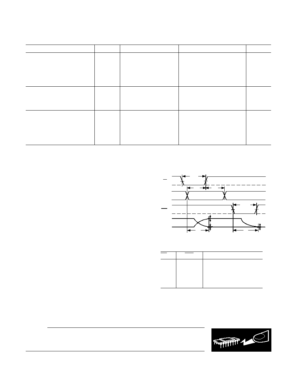
1
0
1
FS
ZS
DB11–0
VOUT
t
CEW
t
DS
t
DH
DATA VALID
t
CLRW
t
S
t
S
±1 LSB
ERROR BAND
CE
CLR
Figure 2. Timing Diagram
Table I. Control Logic Truth Table
CE
CLR
DAC Register Function
H
Latched
L
H
Transparent
↑ +
H
Latched with New Data
X
L
Loaded with All Zeros
H
↑ +
Latched All Zeros
↑ + Positive Logic Transition; X Don't Care.
REV. A
–3–
(@ VDD = +5.0 V
5%, RL = No Load, TA = +25 C, applies to part number DAC8562GBC only,
unless otherwise noted)
DAC8562
相关PDF资料 |
PDF描述 |
|---|---|
| LTC1596BCN | IC D/A CONV 16BIT MLTPLYNG 16DIP |
| VI-B21-MY-B1 | CONVERTER MOD DC/DC 12V 50W |
| LTC1596-1BCN | IC D/A CONV 16BIT MLTPLYNG 16DIP |
| VI-23Z-MX-B1 | CONVERTER MOD DC/DC 2V 30W |
| LTC1595CIS8#PBF | IC D/A CONV 16BIT MULTPLYNG8SOIC |
相关代理商/技术参数 |
参数描述 |
|---|---|
| DAC8562FS-REEL | 功能描述:IC DAC 12BIT PARALLEL 5V 20-SOIC RoHS:否 类别:集成电路 (IC) >> 数据采集 - 数模转换器 系列:- 产品培训模块:Data Converter Fundamentals DAC Architectures 标准包装:750 系列:- 设置时间:7µs 位数:16 数据接口:并联 转换器数目:1 电压电源:双 ± 功率耗散(最大):100mW 工作温度:0°C ~ 70°C 安装类型:表面贴装 封装/外壳:28-LCC(J 形引线) 供应商设备封装:28-PLCC(11.51x11.51) 包装:带卷 (TR) 输出数目和类型:1 电压,单极;1 电压,双极 采样率(每秒):143k |
| DAC8562FSZ | 功能描述:IC DAC 12BIT PARALLEL 5V 20SOIC RoHS:是 类别:集成电路 (IC) >> 数据采集 - 数模转换器 系列:- 标准包装:1 系列:- 设置时间:4.5µs 位数:12 数据接口:串行,SPI? 转换器数目:1 电压电源:单电源 功率耗散(最大):- 工作温度:-40°C ~ 125°C 安装类型:表面贴装 封装/外壳:8-SOIC(0.154",3.90mm 宽) 供应商设备封装:8-SOICN 包装:剪切带 (CT) 输出数目和类型:1 电压,单极;1 电压,双极 采样率(每秒):* 其它名称:MCP4921T-E/SNCTMCP4921T-E/SNRCTMCP4921T-E/SNRCT-ND |
| DAC8562FSZ-REEL | 功能描述:IC DAC 12BIT PARALLEL 5V 20-SOIC RoHS:是 类别:集成电路 (IC) >> 数据采集 - 数模转换器 系列:- 标准包装:47 系列:- 设置时间:2µs 位数:14 数据接口:并联 转换器数目:1 电压电源:单电源 功率耗散(最大):55µW 工作温度:-40°C ~ 85°C 安装类型:表面贴装 封装/外壳:28-SSOP(0.209",5.30mm 宽) 供应商设备封装:28-SSOP 包装:管件 输出数目和类型:1 电流,单极;1 电流,双极 采样率(每秒):* |
| DAC8562GBC | 制造商:AD 制造商全称:Analog Devices 功能描述:+5 Volt, Parallel Input Complete 12-Bit DAC |
| DAC8562SDGSR | 功能描述:数模转换器- DAC 16B,Dual,Lo Pwr Ultra-Lo Glitch DAC RoHS:否 制造商:Texas Instruments 转换器数量:1 DAC 输出端数量:1 转换速率:2 MSPs 分辨率:16 bit 接口类型:QSPI, SPI, Serial (3-Wire, Microwire) 稳定时间:1 us 最大工作温度:+ 85 C 安装风格:SMD/SMT 封装 / 箱体:SOIC-14 封装:Tube |
发布紧急采购,3分钟左右您将得到回复。