- 您现在的位置:买卖IC网 > PDF目录170654 > DAC8820ICDBG4 (TEXAS INSTRUMENTS INC) PARALLEL, WORD INPUT LOADING, 0.5 us SETTLING TIME, 16-BIT DAC, PDSO28 PDF资料下载
参数资料
| 型号: | DAC8820ICDBG4 |
| 厂商: | TEXAS INSTRUMENTS INC |
| 元件分类: | DAC |
| 英文描述: | PARALLEL, WORD INPUT LOADING, 0.5 us SETTLING TIME, 16-BIT DAC, PDSO28 |
| 封装: | GREEN, PLASTIC, SSOP-28 |
| 文件页数: | 4/22页 |
| 文件大小: | 1216K |
| 代理商: | DAC8820ICDBG4 |
www.ti.com
TotalHarmonicDistortion(dB)
45
55
65
75
85
95
105
115
-
10
100
1000
10k 20k 30k
Frequency(Hz)
500kHzFilter
80kHzFilter
30kHzFilter
CodeFFFFh
V
=6V
REF
RMS
1
V
=+5V
DD
OneOPA627
C =20pF
THEORY OF OPERATION
R
I
OUT
GND
V
REF
2R
R
FB
V
OUT
+ *VREF
D
65536
(1)
SBAS358D – AUGUST 2005 – REVISED FEBRUARY 2008
TYPICAL CHARACTERISTICS (continued)
At TA = +25°C, unless otherwise noted.
UNIPOLAR MULTIPLYING MODE THD
vs FREQUENCY
Figure 37.
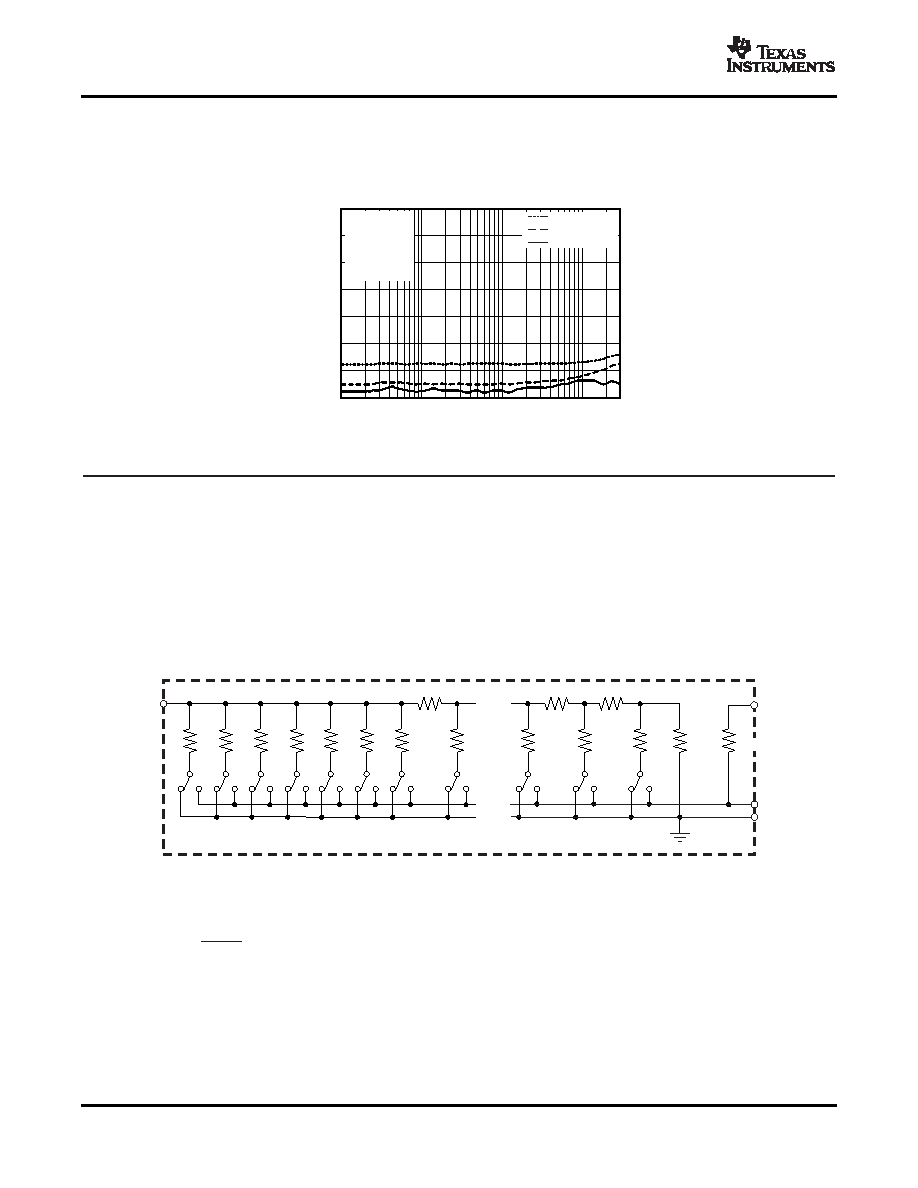
The DAC8820 is a multiplying, single-channel current output, 16-bit DAC. The architecture, illustrated in
Figure 38, is an R-2R ladder configuration with the three MSBs segmented. Each 2R leg of the ladder is either
switched to GND or to the IOUT terminal. The IOUT terminal of the DAC is held at a virtual GND potential by the
use of an external I/V converter op amp. The R-2R ladder is connected to an external reference input (VREF) that
determines the DAC full-scale current. The R-2R ladder presents a code independent load impedance to the
external reference of 6 k
±25%. The external reference voltage can vary in a range of –15 V to +15 V, thus
providing bipolar IOUT current operation. By using an external I/V converter op amp and the RFB resistor in the
DAC8820, an output voltage range of –VREF to +VREF can be generated.
Figure 38. Equivalent R-2R DAC Circuit
Each DAC code determines the 2R-leg switch position to either GND or IOUT. The external I/V converter op amp
noise gain will also change because the DAC output impedance (as seen looking into the IOUT terminal) changes
versus code. Because of this, the external I/V converter op amp must have a sufficiently low offset voltage such
that the amplifier offset is not modulated by the DAC IOUT terminal impedance change. External op amps with
large offset voltages can produce INL errors in the transfer function of the DAC8820 because of offset
modulation versus DAC code. For best linearity performance of the DAC8820, an op amp (OPA277) is
12
Copyright 2005–2008, Texas Instruments Incorporated
Product Folder Link(s): DAC8820
相关PDF资料 |
PDF描述 |
|---|---|
| DAC8820IBDBG4 | PARALLEL, WORD INPUT LOADING, 0.5 us SETTLING TIME, 16-BIT DAC, PDSO28 |
| DAC8840FSZ-REEL | QUAD, SERIAL INPUT LOADING, 3.5 us SETTLING TIME, 8-BIT DAC, PDSO24 |
| DAC | D SUBMINIATURE CONNECTOR, PLUG |
| DEC | D SUBMINIATURE CONNECTOR, PLUG |
| DDC | D SUBMINIATURE CONNECTOR, PLUG |
相关代理商/技术参数 |
参数描述 |
|---|---|
| DAC8820ICDBR | 功能描述:数模转换器- DAC 16-Bit Parallel Inp RoHS:否 制造商:Texas Instruments 转换器数量:1 DAC 输出端数量:1 转换速率:2 MSPs 分辨率:16 bit 接口类型:QSPI, SPI, Serial (3-Wire, Microwire) 稳定时间:1 us 最大工作温度:+ 85 C 安装风格:SMD/SMT 封装 / 箱体:SOIC-14 封装:Tube |
| DAC8820ICDBRG4 | 功能描述:数模转换器- DAC 16-Bit Parallel Inp RoHS:否 制造商:Texas Instruments 转换器数量:1 DAC 输出端数量:1 转换速率:2 MSPs 分辨率:16 bit 接口类型:QSPI, SPI, Serial (3-Wire, Microwire) 稳定时间:1 us 最大工作温度:+ 85 C 安装风格:SMD/SMT 封装 / 箱体:SOIC-14 封装:Tube |
| DAC8822 | 制造商:BB 制造商全称:BB 功能描述:16-Bit, Dual, Parallel Input, Multiplying Digital-to-Analog Converter |
| DAC8822_07 | 制造商:BB 制造商全称:BB 功能描述:16-Bit, Dual, Parallel Input, Multiplying Digital-to-Analog Converter |
| DAC8822QB | 制造商:BB 制造商全称:BB 功能描述:16-Bit, Dual, Parallel Input, Multiplying Digital-to-Analog Converter |
发布紧急采购,3分钟左右您将得到回复。