- 您现在的位置:买卖IC网 > PDF目录17032 > DC1082A-A (Linear Technology)BOARD SAR ADC LTC1407A-1 PDF资料下载
参数资料
| 型号: | DC1082A-A |
| 厂商: | Linear Technology |
| 文件页数: | 20/24页 |
| 文件大小: | 0K |
| 描述: | BOARD SAR ADC LTC1407A-1 |
| 软件下载: | QuikEval II System |
| 设计资源: | DC1082A Design File DC1082A Schematic |
| 标准包装: | 1 |
| 系列: | QuikEval-II™ |
| ADC 的数量: | 1 |
| 位数: | 14 |
| 采样率(每秒): | 3M |
| 数据接口: | 串行,SPI? |
| 输入范围: | ±1.25 V |
| 已用 IC / 零件: | LTC1407-1 |
| 已供物品: | 板 |
| 相关产品: | LTC1407HMSE#PBF-ND - IC ADC 12BIT 3MSPS 10-MSOP LTC1407HMSE#TRPBF-ND - IC ADC 12BIT 3MSPS 10-MSOP LTC1407AHMSE#TRPBF-ND - IC ADC 14BIT 3MSPS 10-MSOP LTC1407AHMSE#PBF-ND - IC ADC 14BIT 3MSPS 10-MSOP LTC1407AIMSE#PBF-ND - IC ADC 14BIT 3MSPS 10-MSOP LTC1407AIMSE-1#PBF-ND - IC ADC 14BIT 3MSPS 10-MSOP LTC1407CMSE-1#PBF-ND - IC ADC 12BIT 3MSPS 10-MSOP LTC1407CMSE#PBF-ND - IC ADC 12BIT 3MSPS 10-MSOP LTC1407ACMSE#PBF-ND - IC ADC 14BIT 3MSPS 10-MSOP LTC1407ACMSE-1#PBF-ND - IC ADC 14BIT 3MSPS 10-MSOP 更多... |
LTC1407/LTC1407A
5
1407fb
Note 1: Stresses beyond those listed under Absolute Maximum Ratings
may cause permanent damage to the device. Exposure to any Absolute
Maximum Rating condition for extended periods may affect device
reliability and lifetime.
Note 2: All voltage values are with respect to ground GND.
Note 3: When these pins are taken below GND or above VDD, they will be
clamped by internal diodes. This product can handle input currents greater
than 100mA below GND or greater than VDD without latchup.
Note 4: Offset and range specications apply for a single-ended CH0+ or CH1+
input with CH0– or CH1– grounded and using the internal 2.5V reference.
Note 5: Integral linearity is tested with an external 2.55V reference and is
dened as the deviation of a code from the straight line passing through
the actual endpoints of a transfer curve. The deviation is measured from
the center of quantization band.
Note 6: Guaranteed by design, not subject to test.
Note 7: Recommended operating conditions.
Note 8: The analog input range is dened for the voltage difference
between CH0+ and CH0– or CH1+ and CH1–.
Note 9: The absolute voltage at CH0+, CH0–, CH1+ and CH1– must be
within this range.
Note 10: If less than 3ns is allowed, the output data will appear one
clock cycle later. It is best for CONV to rise half a clock before SCK, when
running the clock at rated speed.
Note 11: Not the same as aperture delay. Aperture delay (1ns) is the
difference between the 2.2ns delay through the sample-and-hold and the
1.2ns CONV to Hold mode delay.
Note 12: The rising edge of SCK is guaranteed to catch the data coming
out into a storage latch.
Note 13: The time period for acquiring the input signal is started by the
32nd rising clock and it is ended by the rising edge of CONV.
Note 14: The internal reference settles in 2ms after it wakes up from Sleep
mode with one or more cycles at SCK and a 10μF capacitive load.
Note 15: The full power bandwidth is the frequency where the output code
swing drops by 3dB with a 2.5VP-P input sine wave.
Note 16: Maximum clock period guarantees analog performance during
conversion. Output data can be read with an arbitrarily long clock period.
Note 17: The LTC1407A is measured and specied with 14-bit resolution
(1LSB = 152μV) and the LTC1407 is measured and specied with 12-bit
resolution (1LSB = 610μV).
SYMBOL
PARAMETER
CONDITIONS
MIN
TYP
MAX
UNITS
t7
32nd SCK
↑ to CONV↑ Interval (Affects Acquisition Period)
(Notes 6, 7, 13)
45
ns
t8
Minimum Delay from SCK to Valid Bits 0 Through 11
(Notes 6, 12)
8
ns
t9
SCK to Hi-Z at SDO
(Notes 6, 12)
6
ns
t10
Previous SDO Bit Remains Valid After SCK
(Notes 6, 12)
2
ns
t12
VREF Settling Time After Sleep-to-Wake Transition
(Notes 6, 14)
2
ms
TIMING CHARACTERISTICS The l denotes the specications which apply over the full operating temperature
range, otherwise specications are at TA = 25°C. VDD = 3V.
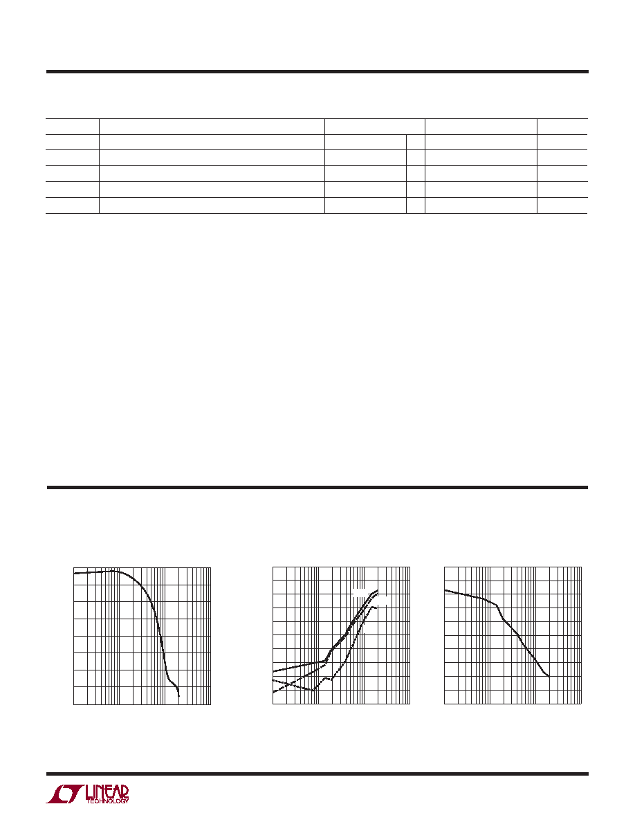
TYPICAL PERFORMANCE CHARACTERISTICS
ENOBs and SINAD
vs Input Sinewave Frequency
THD, 2nd and 3rd
vs Input Frequency
SFDR vs Input Frequency
VDD = 3V, TA = 25°C (LTC1407A)
FREQUENCY (MHz)
0.1
10.0
ENOBs
(BITS)
SINAD
(dB)
11.0
12.0
1
10
100
1407 G01
9.0
9.5
10.5
11.5
8.5
8.0
62
68
74
56
59
65
71
53
50
FREQUENCY (MHz)
0.1
–80
THD,
2nd,
3rd
(dB)
–74
–68
–62
–56
1
10
100
1407 G02
–86
–92
–98
–104
–50
–44
THD
3rd
2nd
FREQUENCY (MHz)
0.1
68
SFDR
(dB)
56
44
1
10
100
1407 G19
80
74
62
50
86
92
98
104
相关PDF资料 |
PDF描述 |
|---|---|
| FPF2313LMPX | IC LOAD SW 2CH ADJ CURR 8-MLP |
| DC1813A-F | BOARD SAR ADC LTC2368-18 |
| DC1813A-C | BOARD SAR ADC LTC2367-16 |
| ADR433ARMZ-REEL7 | IC VREF SERIES PREC 3V 8-MSOP |
| ECE-V1CA471UP | CAP ALUM 470UF 16V 20% SMD |
相关代理商/技术参数 |
参数描述 |
|---|---|
| DC1082A-B | 功能描述:BOARD SAR ADC LTC1407A RoHS:是 类别:编程器,开发系统 >> 评估板 - 模数转换器 (ADC) 系列:QuikEval-II™ 产品培训模块:Obsolescence Mitigation Program 标准包装:1 系列:- ADC 的数量:1 位数:12 采样率(每秒):94.4k 数据接口:USB 输入范围:±VREF/2 在以下条件下的电源(标准):- 工作温度:-40°C ~ 85°C 已用 IC / 零件:MAX11645 已供物品:板,软件 |
| DC1082A-C | 功能描述:BOARD SAR ADC LTC1403A-1 RoHS:是 类别:编程器,开发系统 >> 评估板 - 模数转换器 (ADC) 系列:QuikEval-II™ 产品培训模块:Obsolescence Mitigation Program 标准包装:1 系列:- ADC 的数量:1 位数:12 采样率(每秒):94.4k 数据接口:USB 输入范围:±VREF/2 在以下条件下的电源(标准):- 工作温度:-40°C ~ 85°C 已用 IC / 零件:MAX11645 已供物品:板,软件 |
| DC1082A-D | 功能描述:BOARD SAR ADC LTC1403A RoHS:是 类别:编程器,开发系统 >> 评估板 - 模数转换器 (ADC) 系列:QuikEval-II™ 产品培训模块:Obsolescence Mitigation Program 标准包装:1 系列:- ADC 的数量:1 位数:12 采样率(每秒):94.4k 数据接口:USB 输入范围:±VREF/2 在以下条件下的电源(标准):- 工作温度:-40°C ~ 85°C 已用 IC / 零件:MAX11645 已供物品:板,软件 |
| DC1082A-E | 功能描述:BOARD SAR ADC LTC2356-14 RoHS:是 类别:编程器,开发系统 >> 评估板 - 模数转换器 (ADC) 系列:QuikEval-II™ 产品培训模块:Obsolescence Mitigation Program 标准包装:1 系列:- ADC 的数量:1 位数:12 采样率(每秒):94.4k 数据接口:USB 输入范围:±VREF/2 在以下条件下的电源(标准):- 工作温度:-40°C ~ 85°C 已用 IC / 零件:MAX11645 已供物品:板,软件 |
| DC1082A-F | 功能描述:BOARD SAR ADC LTC2355-14 RoHS:是 类别:编程器,开发系统 >> 评估板 - 模数转换器 (ADC) 系列:QuikEval-II™ 产品培训模块:Obsolescence Mitigation Program 标准包装:1 系列:- ADC 的数量:1 位数:12 采样率(每秒):94.4k 数据接口:USB 输入范围:±VREF/2 在以下条件下的电源(标准):- 工作温度:-40°C ~ 85°C 已用 IC / 零件:MAX11645 已供物品:板,软件 |
发布紧急采购,3分钟左右您将得到回复。